- 您现在的位置:买卖IC网 > PDF目录180051 > M-ORSO82G51BM680-DB (LATTICE SEMICONDUCTOR CORP) FPGA, 1296 CLBS, 333000 GATES, PBGA680 PDF资料下载
参数资料
| 型号: | M-ORSO82G51BM680-DB |
| 厂商: | LATTICE SEMICONDUCTOR CORP |
| 元件分类: | FPGA |
| 英文描述: | FPGA, 1296 CLBS, 333000 GATES, PBGA680 |
| 封装: | PLASTIC, FBGA-680 |
| 文件页数: | 116/123页 |
| 文件大小: | 2207K |
| 代理商: | M-ORSO82G51BM680-DB |
第1页第2页第3页第4页第5页第6页第7页第8页第9页第10页第11页第12页第13页第14页第15页第16页第17页第18页第19页第20页第21页第22页第23页第24页第25页第26页第27页第28页第29页第30页第31页第32页第33页第34页第35页第36页第37页第38页第39页第40页第41页第42页第43页第44页第45页第46页第47页第48页第49页第50页第51页第52页第53页第54页第55页第56页第57页第58页第59页第60页第61页第62页第63页第64页第65页第66页第67页第68页第69页第70页第71页第72页第73页第74页第75页第76页第77页第78页第79页第80页第81页第82页第83页第84页第85页第86页第87页第88页第89页第90页第91页第92页第93页第94页第95页第96页第97页第98页第99页第100页第101页第102页第103页第104页第105页第106页第107页第108页第109页第110页第111页第112页第113页第114页第115页当前第116页第117页第118页第119页第120页第121页第122页第123页
Lattice Semiconductor
ORCA ORSO82G5 Data Sheet
92
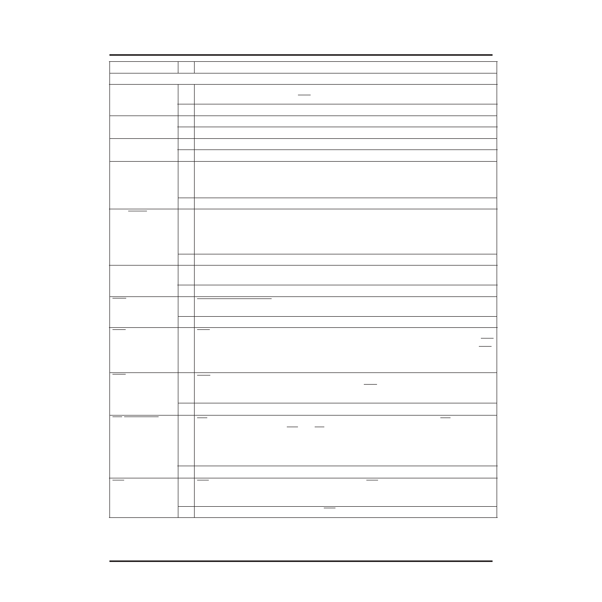
Special-Purpose Pins
M[3:0]
I
During powerup and initialization, M0—M3 are used to select the conguration mode with their val-
ues latched on the rising edge of INIT. During conguration, a pull-up is enabled.
I/O
After conguration, these pins are user-programmable I/O.*
PLL_CK[0:7][TC]
I
Semi-dedicated PLL clock pins. During conguration they are 3-stated with a pull up.
I/O
These pins are user-programmable I/O pins if not used by PLLs after conguration.
P[TBLR]CLK[1:0][TC]
I
Pins dedicated for the primary clock. Input pins on the middle of each side with differential pairing.
I/O
After conguration these pins are user programmable I/O, if not used for clock inputs.
TDI, TCK, TMS
I
If boundary-scan is used, these pins are test data in, test clock, and test mode select inputs. If
boundary-scan is not selected, all boundary-scan functions are inhibited once conguration is com-
plete. Even if boundary-scan is not used, either TCK or TMS must be held at logic 1 during congu-
ration. Each pin has a pull-up enabled during conguration.
I/O
After conguration, these pins are user-programmable I/O if boundary scan is not used.*
RDY/BUSY/RCLK
O
During conguration in asynchronous peripheral mode, RDY/RCLK indicates another byte can be
written to the FPGA. If a read operation is done when the device is selected, the same status is
also available on D7 in asynchronous peripheral mode.
During the master parallel conguration mode, RCLK is a read output signal to an external memory.
This output is not normally used.
I/O
After conguration this pin is a user-programmable I/O pin.*
HDC
O
High During Conguration is output high until conguration is complete. It is used as a control out-
put, indicating that conguration is not complete.
I/O
After conguration, this pin is a user-programmable I/O pin.*
LDC
O
Low During Conguration
is output low until conguration is complete. It is used as a control output,
indicating that conguration is not complete.
I/O
After conguration, this pin is a user-programmable I/O pin.*
INIT
I/O
INIT
is a bidirectional signal before and during conguration. During conguration, a pull-up is
enabled, but an external pull-up resistor is recommended. As an active-low open-drain output, INIT
is held low during power stabilization and internal clearing of memory. As an active-low input, INIT
holds the FPGA in the wait-state before the start of conguration.
After conguration, this pin is a user-programmable I/O pin.*
CS0, CS1
I
CS0
and CS1 are used in the asynchronous peripheral, slave parallel, and microprocessor
conguration modes. The FPGA is selected when CS0 is low and CS1 is high. During con-
guration, a pull-up is enabled.
I/O
After conguration, if MPI is not used, these pins are user-programmable I/O pins.*
RD/MPI_STRB
I
RD
is used in the asynchronous peripheral conguration mode. A low on RD changes
D[7:3] into a status output. WR and RD should not be used simultaneously. If they are, the
write strobe overrides.
This pin is also used as the MPI data transfer strobe. As a status indication, a high
indicates ready, and a low indicates busy.
I/O After conguration, if the MPI is not used, this pin is a user-programmable I/O pin.*
WR/MPI_RW
I
WR is used in asynchronous peripheral mode. A low on WR transfers data on D[7:0] to the FPGA.
In MPI mode, a high on MPI_RW allows a read from the data bus, while a low causes a write trans-
fer to the FPGA.
I/O
After conguration, if the MPI is not used, WR/MPI_RW is a user-programmable I/O pin.*
Symbol
I/O
Description
* The FPGA States of Operation section contains more information on how to control these signals during start-up. The timing of DONE release
is controlled by one set of bit stream options, and the timing of the simultaneous release of all other conguration pins (and the activation of all
user I/Os) is controlled by a second set of options.
相关PDF资料 |
PDF描述 |
|---|---|
| M-ORSO82G52BM680-DB | FPGA, 1296 CLBS, 333000 GATES, PBGA680 |
| M-ORT82G51BM680-DB | FPGA, 1296 CLBS, 333000 GATES, PBGA680 |
| M-ORT82G52BM680-DB | FPGA, 1296 CLBS, 333000 GATES, PBGA680 |
| M.PI-1R1D12 | 1 ELEMENT, 1.1 uH, GENERAL PURPOSE INDUCTOR, SMD |
| M01-014-1452PA | 14 CONTACT(S), MALE, RIGHT ANGLE TELECOM AND DATACOM CONNECTOR, SOLDER |
相关代理商/技术参数 |
参数描述 |
|---|---|
| MORTAR-44LB | 制造商:3M Electronic Products Division 功能描述:3M(TM) FIRE BARRIER MORTAR, 44 98040056073 制造商:3M Electronic Products Division 功能描述:Fire Barrier 44 lb Bag |
| MO-RX3930 | 制造商:未知厂家 制造商全称:未知厂家 功能描述:FSK RECEIVER MODULE |
| MO-RX3930-FS | 制造商:未知厂家 制造商全称:未知厂家 功能描述:FSK RECEIVER MODULE |
| MO-RX3930-FS315M | 制造商:未知厂家 制造商全称:未知厂家 功能描述:FSK RECEIVER MODULE |
| MO-RX3930-FS434M | 制造商:未知厂家 制造商全称:未知厂家 功能描述:FSK RECEIVER MODULE |
发布紧急采购,3分钟左右您将得到回复。