- 您现在的位置:买卖IC网 > Datasheet目录368 > W631GG6KB-15 (Winbond Electronics)IC DDR3 SDRAM 1GBIT 96WBGA Datasheet资料下载
参数资料
| 型号: | W631GG6KB-15 |
| 厂商: | Winbond Electronics |
| 文件页数: | 30/159页 |
| 文件大小: | 0K |
| 描述: | IC DDR3 SDRAM 1GBIT 96WBGA |
| 标准包装: | 200 |
| 格式 - 存储器: | RAM |
| 存储器类型: | DDR3 SDRAM |
| 存储容量: | 1G(64M x 16) |
| 速度: | 667MHz |
| 接口: | 并联 |
| 电源电压: | 1.425 V ~ 1.575 V |
| 工作温度: | 0°C ~ 85°C |
| 封装/外壳: | 96-TFBGA |
| 供应商设备封装: | 96-WBGA(9x13) |
| 包装: | 托盘 |
第1页第2页第3页第4页第5页第6页第7页第8页第9页第10页第11页第12页第13页第14页第15页第16页第17页第18页第19页第20页第21页第22页第23页第24页第25页第26页第27页第28页第29页当前第30页第31页第32页第33页第34页第35页第36页第37页第38页第39页第40页第41页第42页第43页第44页第45页第46页第47页第48页第49页第50页第51页第52页第53页第54页第55页第56页第57页第58页第59页第60页第61页第62页第63页第64页第65页第66页第67页第68页第69页第70页第71页第72页第73页第74页第75页第76页第77页第78页第79页第80页第81页第82页第83页第84页第85页第86页第87页第88页第89页第90页第91页第92页第93页第94页第95页第96页第97页第98页第99页第100页第101页第102页第103页第104页第105页第106页第107页第108页第109页第110页第111页第112页第113页第114页第115页第116页第117页第118页第119页第120页第121页第122页第123页第124页第125页第126页第127页第128页第129页第130页第131页第132页第133页第134页第135页第136页第137页第138页第139页第140页第141页第142页第143页第144页第145页第146页第147页第148页第149页第150页第151页第152页第153页第154页第155页第156页第157页第158页第159页
�� �
�
�W631GG6KB�
�8.9�
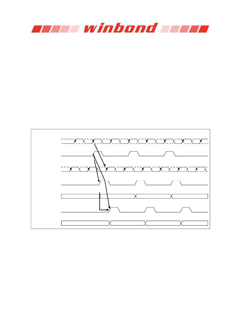
�Write� Leveling�
�For� better� signal� integrity,� the� DDR3� memory� module� adopted� fly-by� topology� for� the� commands,�
�addresses,� control� signals,� and� clocks.� The� fly-by� topology� has� benefits� from� reducing� number� of�
�stubs� and� their� length,� but� it� also� causes� flight� time� skew� between� clock� and� strobe� at� every� DRAM� on�
�the� DIMM.� This� makes� it� difficult� for� the� Controller� to� maintain� t� DQSS� ,� t� DSS� ,� and� t� DSH� specification.�
�Therefore,� the� DDR3� SDRAM� supports� a� ?write� leveling‘� feature� to� allow� the� controller� to� compensate�
�for� skew.�
�The� memory� controller� can� use� the� ?write� leveling‘� feature� and� feedback� from� the� DDR3� SDRAM� to�
�adjust� the� DQS� -� DQS#� to� CK� -� CK#� relationship.� The� memory� controller� involved� in� the� leveling� must�
�have� adjustable� delay� setting� on� DQS� -� DQS#� to� align� the� rising� edge� of� DQS� -� DQS#� with� that� of� the�
�clock� at� the� DRAM� pin.� The� DRAM� asynchronously� feeds� back� CK� -� CK#,� sampled� with� the� rising�
�edge� of� DQS� -� DQS#,� through� the� DQ� bus.� The� controller� repeatedly� delays� DQS� -� DQS#� until� a�
�transition� from� 0� to� 1� is� detected.� The� DQS� -� DQS#� delay� established� though� this� exercise� would�
�ensure� t� DQSS� specification.�
�Besides� t� DQSS� ,� t� DSS� and� t� DSH� specification� also� needs� to� be� fulfilled.� One� way� to� achieve� this� is� to�
�combine� the� actual� t� DQSS� in� the� application� with� an� appropriate� duty� cycle� and� jitter� on� the� DQS� -�
�DQS#� signals.� Depending� on� the� actual� t� DQSS� in� the� application,� the� actual� values� for� t� DQSL� and� t� DQSH�
�may� have� to� be� better� than� the� absolute� limits� provided� in� section� 9.16� “� AC� Characteristics� ”� in� order�
�to� satisfy� t� DSS� and� tDSH� specification.� A� conceptual� timing� of� this� scheme� is� shown� in� Figure� 13.�
�T0�
�T1�
�T2�
�T3�
�T4�
�T5�
�T6�
�T7�
�Source�
�CK#�
�CK�
�Diff_DQS�
�Destination�
�CK#�
�CK�
�Tn�
�T0�
�T1�
�T2�
�T3�
�T4�
�T5�
�T6�
�Diff_DQS�
�DQ�
�0� or� 1�
�0�
�0�
�0�
�Push� DQS� to� capture� 0-1�
�Diff_DQS�
�transition�
�DQ�
�0� or� 1�
�1�
�1�
�1�
�Figure� 13� –� Write� Leveling� Concept�
�DQS� -� DQS#� driven� by� the� controller� during� leveling� mode� must� be� terminated� by� the� DRAM� based� on�
�ranks� populated.� Similarly,� the� DQ� bus� driven� by� the� DRAM� must� also� be� terminated� at� the� controller.�
�One� or� more� data� bits� should� carry� the� leveling� feedback� to� the� controller� across� the� DRAM�
�configurations� x4,� x8� and� x16.� On� a� x16� device,� both� byte� lanes� should� be� leveled� independently.�
�Therefore,� a� separate� feedback� mechanism� should� be� available� for� each� byte� lane.� The� upper� data�
�bits� should� provide� the� feedback� of� the� upper� Diff_DQS(Diff_UDQS)� to� clock� relationship� whereas� the�
�lower� data� bits� would� indicate� the� lower� Diff_DQS(Diff_LDQS)� to� clock� relationship.�
�Publication� Release� Date:� Dec.� 09,� 2013�
�Revision� A05�
�-� 30� -�
�相关PDF资料 |
PDF描述 |
|---|---|
| W9412G6IH-5 | IC DDR-400 SDRAM 128MB 66TSSOPII |
| W9412G6JH-5I | IC DDR SDRAM 128MBIT 66TSOPII |
| W9425G6EH-5 | IC DDR-400 SDRAM 256MB 66TSSOPII |
| W9425G6JH-5I | IC DDR SDRAM 256MBIT 66TSOPII |
| W947D2HBJX5E | IC LPDDR SDRAM 128MBIT 90VFBGA |
相关代理商/技术参数 |
参数描述 |
|---|---|
| W631GG8KB-11 | 制造商:Winbond Electronics Corp 功能描述:IC DDR3 SDRAM 1GBIT 制造商:Winbond Electronics Corp 功能描述:IC DDR3 SDRAM 1GBIT 78WBGA |
| W631GG8KB-12 | 制造商:Winbond Electronics Corp 功能描述:DRAM Chip DDR3 SDRAM 1G-Bit 128Mx8 1.5V 制造商:Winbond Electronics Corp 功能描述:IC DDR3 SDRAM 1GBIT 制造商:Winbond Electronics Corp 功能描述:IC DDR3 SDRAM 1GBIT 78WBGA |
| W631GG8KB-15 | 制造商:Winbond Electronics Corp 功能描述:IC DDR3 SDRAM 1GBIT 制造商:Winbond Electronics Corp 功能描述:IC DDR3 SDRAM 1GBIT 78WBGA |
| W632 | 制造商:LUMINIS 制造商全称:LUMINIS 功能描述:Wall mount |
| W632GG6KB-11 | 制造商:Winbond Electronics Corp 功能描述:IC DDR3 SDRAM 2GBIT 96WBGA |
发布紧急采购,3分钟左右您将得到回复。