- 您现在的位置:买卖IC网 > Datasheet目录368 > W631GG6KB-15 (Winbond Electronics)IC DDR3 SDRAM 1GBIT 96WBGA Datasheet资料下载
参数资料
| 型号: | W631GG6KB-15 |
| 厂商: | Winbond Electronics |
| 文件页数: | 99/159页 |
| 文件大小: | 0K |
| 描述: | IC DDR3 SDRAM 1GBIT 96WBGA |
| 标准包装: | 200 |
| 格式 - 存储器: | RAM |
| 存储器类型: | DDR3 SDRAM |
| 存储容量: | 1G(64M x 16) |
| 速度: | 667MHz |
| 接口: | 并联 |
| 电源电压: | 1.425 V ~ 1.575 V |
| 工作温度: | 0°C ~ 85°C |
| 封装/外壳: | 96-TFBGA |
| 供应商设备封装: | 96-WBGA(9x13) |
| 包装: | 托盘 |
第1页第2页第3页第4页第5页第6页第7页第8页第9页第10页第11页第12页第13页第14页第15页第16页第17页第18页第19页第20页第21页第22页第23页第24页第25页第26页第27页第28页第29页第30页第31页第32页第33页第34页第35页第36页第37页第38页第39页第40页第41页第42页第43页第44页第45页第46页第47页第48页第49页第50页第51页第52页第53页第54页第55页第56页第57页第58页第59页第60页第61页第62页第63页第64页第65页第66页第67页第68页第69页第70页第71页第72页第73页第74页第75页第76页第77页第78页第79页第80页第81页第82页第83页第84页第85页第86页第87页第88页第89页第90页第91页第92页第93页第94页第95页第96页第97页第98页当前第99页第100页第101页第102页第103页第104页第105页第106页第107页第108页第109页第110页第111页第112页第113页第114页第115页第116页第117页第118页第119页第120页第121页第122页第123页第124页第125页第126页第127页第128页第129页第130页第131页第132页第133页第134页第135页第136页第137页第138页第139页第140页第141页第142页第143页第144页第145页第146页第147页第148页第149页第150页第151页第152页第153页第154页第155页第156页第157页第158页第159页
�� �
�
�W631GG6KB�
�10.3� DC� &� AC� Operating� Conditions�
�10.3.1� Recommended� DC� Operating� Conditions�
�SYM.�
�V� DD�
�V� DDQ�
�R� ZQ�
�PARAMETER�
�Supply� Voltage�
�Supply� Voltage� for� Output�
�External� Calibration� Resistor� connected�
�from� ZQ� ball� to� ground�
�MIN.�
�1.425�
�1.425�
�237.6�
�TYP.�
�1.5�
�1.5�
�240.0�
�MAX.�
�1.575�
�1.575�
�242.4�
�UNIT�
�V�
�V�
�Ω�
�NOTES�
�1,� 2�
�1,� 2�
�3�
�Notes:�
�1.� Under� all� conditions� V� DDQ� must� be� less� than� or� equal� to� V� DD� .�
�2.� V� DDQ� tracks� with� V� DD� .� AC� parameters� are� measured� with� V� DD� and� V� DDQ� tied� together.�
�3.� The� external� calibration� resistor� RZQ� can� be� time-shared� among� DRAMs� in� special� applications.�
�10.4 Input and Output Leakage Currents�
�SYMBOL�
�I� IL�
�I� OL�
�PARAMETER�
�Input� Leakage� Current�
�(0V� ≤� V� IN� ≤� V� DD� )�
�Output� Leakage� Current�
�(Output� disabled,� 0V� ≤� V� OUT� ≤� V� DDQ� )�
�MIN.�
�-2�
�-5�
�MAX.�
�2�
�5�
�UNIT�
�μA�
�μA�
�NOTES�
�1�
�2�
�Notes:�
�1.� All� other� balls� not� under� test� =� 0� V.�
�2.� All� DQ,� DQS� and� DQS#� are� in� high-impedance� mode.�
�10.5� Interface� Test� Conditions�
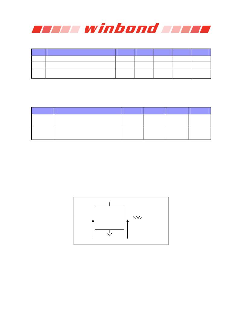
�Figure� 88� represents� the� effective� reference� load� of� 25� ohms� used� in� defining� the� relevant� AC� timing�
�parameters� of� the� device� as� well� as� output� slew� rate� measurements.�
�It� is� not� intended� as� a� precise� representation� of� any� particular� system� environment� or� a� depiction� of�
�the� actual� load� presented� by� a� production� tester.� System� designers� should� use� IBIS� or� other�
�simulation� tools� to� correlate� the� timing� reference� load� to� a� system� environment.� Manufacturers�
�correlate� to� their� production� test� conditions,� generally� one� or� more� coaxial� transmission� lines�
�terminated� at� the� tester� electronics.�
�VDDQ�
�CK,� CK#�
�DUT�
�DQ�
�DQS�
�DQS#�
�25� Ω�
�VTT� =� VDDQ/2�
�Timing� reference� point�
�Figure� 88� –� Reference� Load� for� AC� Timings� and� Output� Slew� Rates�
�The� Timing� Reference� Points� are� the� idealized� input� and� output� nodes� /� terminals� on� the� outside� of� the�
�packaged� SDRAM� device� as� they� would� appear� in� a� schematic� or� an� IBIS� model.�
�The� output� timing� reference� voltage� level� for� single� ended� signals� is� the� cross� point� with� V� TT� .�
�The� output� timing� reference� voltage� level� for� differential� signals� is� the� cross� point� of� the� true� (e.g.�
�DQSL,� DQSU)� and� the� complement� (e.g.� DQSL#,� DQSU#)� signal.�
�Publication� Release� Date:� Dec.� 09,� 2013�
�Revision� A05�
�-� 99� -�
�相关PDF资料 |
PDF描述 |
|---|---|
| W9412G6IH-5 | IC DDR-400 SDRAM 128MB 66TSSOPII |
| W9412G6JH-5I | IC DDR SDRAM 128MBIT 66TSOPII |
| W9425G6EH-5 | IC DDR-400 SDRAM 256MB 66TSSOPII |
| W9425G6JH-5I | IC DDR SDRAM 256MBIT 66TSOPII |
| W947D2HBJX5E | IC LPDDR SDRAM 128MBIT 90VFBGA |
相关代理商/技术参数 |
参数描述 |
|---|---|
| W631GG8KB-11 | 制造商:Winbond Electronics Corp 功能描述:IC DDR3 SDRAM 1GBIT 制造商:Winbond Electronics Corp 功能描述:IC DDR3 SDRAM 1GBIT 78WBGA |
| W631GG8KB-12 | 制造商:Winbond Electronics Corp 功能描述:DRAM Chip DDR3 SDRAM 1G-Bit 128Mx8 1.5V 制造商:Winbond Electronics Corp 功能描述:IC DDR3 SDRAM 1GBIT 制造商:Winbond Electronics Corp 功能描述:IC DDR3 SDRAM 1GBIT 78WBGA |
| W631GG8KB-15 | 制造商:Winbond Electronics Corp 功能描述:IC DDR3 SDRAM 1GBIT 制造商:Winbond Electronics Corp 功能描述:IC DDR3 SDRAM 1GBIT 78WBGA |
| W632 | 制造商:LUMINIS 制造商全称:LUMINIS 功能描述:Wall mount |
| W632GG6KB-11 | 制造商:Winbond Electronics Corp 功能描述:IC DDR3 SDRAM 2GBIT 96WBGA |
发布紧急采购,3分钟左右您将得到回复。