- 您现在的位置:买卖IC网 > Datasheet目录368 > W631GG6KB-15 (Winbond Electronics)IC DDR3 SDRAM 1GBIT 96WBGA Datasheet资料下载
参数资料
| 型号: | W631GG6KB-15 |
| 厂商: | Winbond Electronics |
| 文件页数: | 96/159页 |
| 文件大小: | 0K |
| 描述: | IC DDR3 SDRAM 1GBIT 96WBGA |
| 标准包装: | 200 |
| 格式 - 存储器: | RAM |
| 存储器类型: | DDR3 SDRAM |
| 存储容量: | 1G(64M x 16) |
| 速度: | 667MHz |
| 接口: | 并联 |
| 电源电压: | 1.425 V ~ 1.575 V |
| 工作温度: | 0°C ~ 85°C |
| 封装/外壳: | 96-TFBGA |
| 供应商设备封装: | 96-WBGA(9x13) |
| 包装: | 托盘 |
第1页第2页第3页第4页第5页第6页第7页第8页第9页第10页第11页第12页第13页第14页第15页第16页第17页第18页第19页第20页第21页第22页第23页第24页第25页第26页第27页第28页第29页第30页第31页第32页第33页第34页第35页第36页第37页第38页第39页第40页第41页第42页第43页第44页第45页第46页第47页第48页第49页第50页第51页第52页第53页第54页第55页第56页第57页第58页第59页第60页第61页第62页第63页第64页第65页第66页第67页第68页第69页第70页第71页第72页第73页第74页第75页第76页第77页第78页第79页第80页第81页第82页第83页第84页第85页第86页第87页第88页第89页第90页第91页第92页第93页第94页第95页当前第96页第97页第98页第99页第100页第101页第102页第103页第104页第105页第106页第107页第108页第109页第110页第111页第112页第113页第114页第115页第116页第117页第118页第119页第120页第121页第122页第123页第124页第125页第126页第127页第128页第129页第130页第131页第132页第133页第134页第135页第136页第137页第138页第139页第140页第141页第142页第143页第144页第145页第146页第147页第148页第149页第150页第151页第152页第153页第154页第155页第156页第157页第158页第159页
�� �
�
�W631GG6KB�
�9.2�
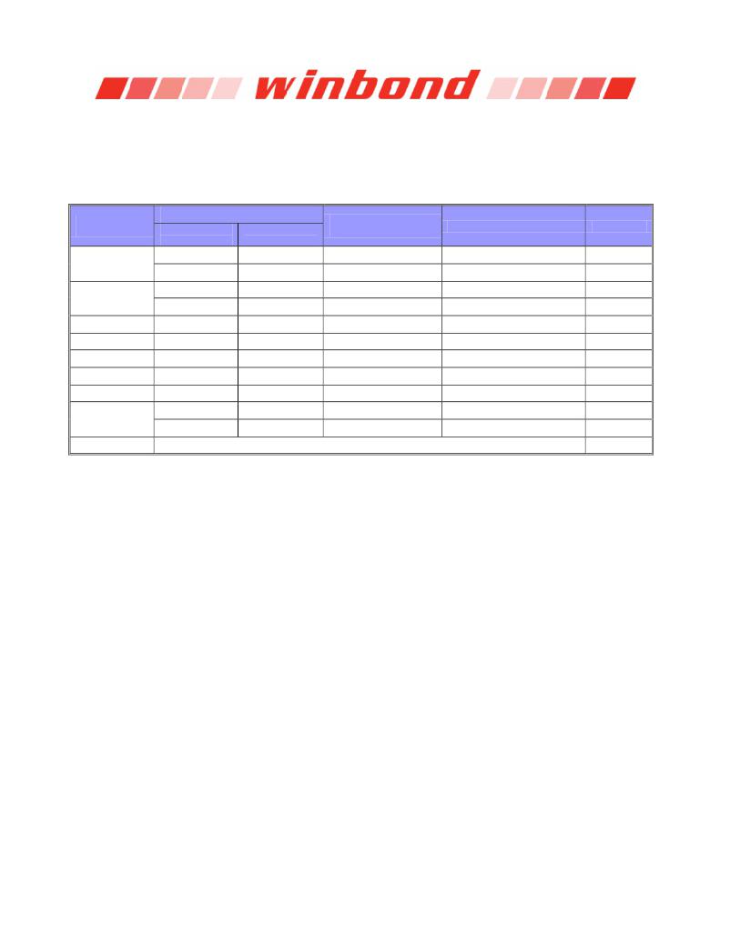
�CKE� Truth� Table�
�Notes� 1-7� apply� to� the� entire� CKE� Truth� Table.�
�For� Power-down� entry� and� exit� parameters� See� 8.17� “� Power-Down� Modes� ”� on� page� 69.�
�CKE� low� is� allowed� only� if� t� MRD� and� t� MOD� are� satisfied.�
�Table� 15� –� CKE� Truth� Table�
�STATE�
�Current� Cycle�
�COMMAND� (N)�
�CURRENT�
�2�
�Previous� Cycle�
�(N-1)�
�CKE�
�1�
�(N)�
�1�
�3�
�RAS#, CAS#, WE#, CS#�
�ACTION� (N)�
�3�
�NOTES�
�Power� Down�
�Self� Refresh�
�Bank(s)� Active�
�Reading�
�Writing�
�Precharging�
�Refreshing�
�All� Banks� Idle�
�L�
�L�
�L�
�L�
�H�
�H�
�H�
�H�
�H�
�H�
�H�
�L�
�H�
�L�
�H�
�L�
�L�
�L�
�L�
�L�
�L�
�L�
�X�
�DESELECT� or� NOP�
�X�
�DESELECT� or� NOP�
�DESELECT� or� NOP�
�DESELECT� or� NOP�
�DESELECT� or� NOP�
�DESELECT� or� NOP�
�DESELECT� or� NOP�
�DESELECT� or� NOP�
�REFRESH�
�Maintain� Power� Down�
�Power� Down� Exit�
�Maintain� Self� Refresh�
�Self� Refresh� Exit�
�Active� Power� Down� Entry�
�Power� Down� Entry�
�Power� Down� Entry�
�Power� Down� Entry�
�Precharge� Power� Down� Entry�
�Precharge� Power� Down� Entry�
�Self� Refresh�
�14,15�
�11,14�
�15,16�
�8,12,16�
�11,13,14�
�11,13,14,17�
�11,13,14,17�
�11,13,14,17�
�11�
�11,13,14,18�
�9,13,18�
�Any� other� state�
�Refer� to� section� 9.1� “� Command� Truth� Table� ”� on� Page� 94� for� more� detail� with� all� command� signals�
�10�
�Notes:�
�1.� CKE� (N)� is� the� logic� state� of� CKE� at� clock� edge� N;� CKE� (N-1)� was� the� state� of� CKE� at� the� previous� clock� edge.�
�2.� Current� state� is� defined� as� the� state� of� the� DDR3� SDRAM� immediately� prior� to� clock� edge� N.�
�3.� COMMAND� (N)� is� the� command� registered� at� clock� edge� N,� and� ACTION� (N)� is� a� result� of� COMMAND� (N),� ODT� is� not�
�included� here.�
�4.� All� states� and� sequences� not� shown� are� illegal� or� reserved� unless� explicitly� described� elsewhere� in� this� document.�
�5.� The� state� of� ODT� does� not� affect� the� states� described� in� this� table.� The� ODT� function� is� not� available� during� Self� Refresh.�
�6.� During� any� CKE� transition� (registration� of� CKE� H->L� or� CKE� L->H)� the� CKE� level� must� be� maintained� until� 1nCK� prior� to�
�t� CKE� min� being� satisfied� (at� which� time� CKE� may� transition� again).�
�7.� DESELECT� and� NOP� are� defined� in� the� Command� Truth� Table.�
�8.� On� Self� Refresh� Exit� DESELECT� or� NOP� commands� must� be� issued� on� every� clock� edge� occurring� during� the� t� XS� period.�
�Read� or� ODT� commands� may� be� issued� only� after� t� XSDLL� is� satisfied.�
�9.� Self� Refresh� mode� can� only� be� entered� from� the� All� Banks� Idle� state.�
�10.� Must� be� a� legal� command� as� defined� in� the� Command� Truth� Table.�
�11.� Valid� commands� for� Power� Down� Entry� and� Exit� are� NOP� and� DESELECT� only.�
�12.� Valid� commands� for� Self� Refresh� Exit� are� NOP� and� DESELECT� only.�
�13.� Self� Refresh� can� not� be� entered� during� Read� or� Write� operations.� For� a� detailed� list� of� restrictions� See� section� 8.16� “� Self-�
�Refresh� Operation� ”� on� page� 67� and� See� section� 8.17� “� Power-Down� Modes� ”� on� page� 69.�
�14.� The� Power� Down� does� not� perform� any� refresh� operations.�
�15.� ―X‖� means� ―� don't� care� ‖� (including� floating� around� V� REF� )� in� Self� Refresh� and� Power� Down.� It� also� applies� to� Address� pins.�
�16.� V� REF� (Both� V� REFDQ� and� V� REFCA� )� must� be� maintained� during� Self� Refresh� operation.� V� REFDQ� supply� may� be� turned� OFF�
�and� V� REFDQ� may� take� any� value� between� V� SS� and� V� DD� during� Self� Refresh� operation,� provided� that� V� REFDQ� is� valid� and�
�stable� prior� to� CKE� going� back� High� and� that� first� Write� operation� or� first� Write� Leveling� Activity� may� not� occur� earlier� than�
�512� nCK� after� exit� from� Self� Refresh.�
�17.� If� all� banks� are� closed� at� the� conclusion� of� the� read,� write� or� precharge� command,� then� Precharge� Power� Down� is� entered,�
�otherwise� Active� Power� Down� is� entered.�
�18.� ?Idle� state‘� is� defined� as� all� banks� are� closed� (t� RP� ,� t� DAL� ,� etc.� satisfied),� no� data� bursts� are� in� progress,� CKE� is� high,� and� all�
�timings� from� previous� operations� are� satisfied� (t� MRD� ,� t� MOD� ,� t� RFC� ,� t� ZQinit� ,� t� ZQ� oper,� t� ZQCS� ,� etc.)� as� well� as� all� Self� Refresh�
�exit� and� Power� Down� Exit� parameters� are� satisfied� (t� XS� ,� t� XP� ,� t� XPDLL� ,� etc).�
�Publication� Release� Date:� Dec.� 09,� 2013�
�Revision� A05�
�-� 96� -�
�相关PDF资料 |
PDF描述 |
|---|---|
| W9412G6IH-5 | IC DDR-400 SDRAM 128MB 66TSSOPII |
| W9412G6JH-5I | IC DDR SDRAM 128MBIT 66TSOPII |
| W9425G6EH-5 | IC DDR-400 SDRAM 256MB 66TSSOPII |
| W9425G6JH-5I | IC DDR SDRAM 256MBIT 66TSOPII |
| W947D2HBJX5E | IC LPDDR SDRAM 128MBIT 90VFBGA |
相关代理商/技术参数 |
参数描述 |
|---|---|
| W631GG8KB-11 | 制造商:Winbond Electronics Corp 功能描述:IC DDR3 SDRAM 1GBIT 制造商:Winbond Electronics Corp 功能描述:IC DDR3 SDRAM 1GBIT 78WBGA |
| W631GG8KB-12 | 制造商:Winbond Electronics Corp 功能描述:DRAM Chip DDR3 SDRAM 1G-Bit 128Mx8 1.5V 制造商:Winbond Electronics Corp 功能描述:IC DDR3 SDRAM 1GBIT 制造商:Winbond Electronics Corp 功能描述:IC DDR3 SDRAM 1GBIT 78WBGA |
| W631GG8KB-15 | 制造商:Winbond Electronics Corp 功能描述:IC DDR3 SDRAM 1GBIT 制造商:Winbond Electronics Corp 功能描述:IC DDR3 SDRAM 1GBIT 78WBGA |
| W632 | 制造商:LUMINIS 制造商全称:LUMINIS 功能描述:Wall mount |
| W632GG6KB-11 | 制造商:Winbond Electronics Corp 功能描述:IC DDR3 SDRAM 2GBIT 96WBGA |
发布紧急采购,3分钟左右您将得到回复。