- 您现在的位置:买卖IC网 > PDF目录1916 > DS34S132GN+ (Maxim Integrated Products)IC TDM OVER PACKET 676-BGA PDF资料下载
参数资料
| 型号: | DS34S132GN+ |
| 厂商: | Maxim Integrated Products |
| 文件页数: | 121/194页 |
| 文件大小: | 0K |
| 描述: | IC TDM OVER PACKET 676-BGA |
| 产品培训模块: | Lead (SnPb) Finish for COTS Obsolescence Mitigation Program |
| 标准包装: | 40 |
| 功能: | TDM-over-Packet(TDMoP) |
| 接口: | TDMoP |
| 电路数: | 1 |
| 电源电压: | 1.8V, 3.3V |
| 工作温度: | -40°C ~ 85°C |
| 安装类型: | 表面贴装 |
| 封装/外壳: | 676-BGA |
| 供应商设备封装: | 676-PBGA(27x27) |
| 包装: | 管件 |
| 其它名称: | 90-34S13+2N0 |
第1页第2页第3页第4页第5页第6页第7页第8页第9页第10页第11页第12页第13页第14页第15页第16页第17页第18页第19页第20页第21页第22页第23页第24页第25页第26页第27页第28页第29页第30页第31页第32页第33页第34页第35页第36页第37页第38页第39页第40页第41页第42页第43页第44页第45页第46页第47页第48页第49页第50页第51页第52页第53页第54页第55页第56页第57页第58页第59页第60页第61页第62页第63页第64页第65页第66页第67页第68页第69页第70页第71页第72页第73页第74页第75页第76页第77页第78页第79页第80页第81页第82页第83页第84页第85页第86页第87页第88页第89页第90页第91页第92页第93页第94页第95页第96页第97页第98页第99页第100页第101页第102页第103页第104页第105页第106页第107页第108页第109页第110页第111页第112页第113页第114页第115页第116页第117页第118页第119页第120页当前第121页第122页第123页第124页第125页第126页第127页第128页第129页第130页第131页第132页第133页第134页第135页第136页第137页第138页第139页第140页第141页第142页第143页第144页第145页第146页第147页第148页第149页第150页第151页第152页第153页第154页第155页第156页第157页第158页第159页第160页第161页第162页第163页第164页第165页第166页第167页第168页第169页第170页第171页第172页第173页第174页第175页第176页第177页第178页第179页第180页第181页第182页第183页第184页第185页第186页第187页第188页第189页第190页第191页第192页第193页第194页
DS34S132 DATA SHEET
19-4750; Rev 1; 07/11
32 of 194
9.2 TDM Port Functions
The S132 includes 32 TDM Ports. Each TDM Port can be used to support a T1, E1 or any slower TDM data
stream. Each TDM Port uses a serial clock and data interface. The high level functions include:
Structured & Unstructured Formats
T1, E1 and slower TDM Port Line Rates
T1SF, T1ESF and E1 Multi-frame Formats
N x 64 Kb/s PW Packet Payload Rates
With & without CAS Signaling
DS0 Timeslot Assignment
CPU Monitor and Control of CAS Signaling
CPU Control for Data Conditioning
TDM Port Timing
From Recovered or External Time References
Adaptive & Differential Clock Recovery
Generates Differential & Absolute Timestamps
TDM Port, Timeslot and PW Loopbacks
BERT Diagnostics
9.2.1 TDM Port Related Input and Output Clocks
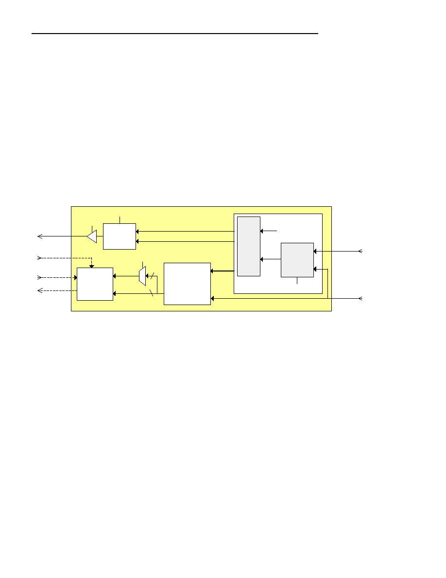
The TDM Port Input and Output Clocks are identified in Figure 9-7.
Figure 9-7. TDM Port Input and Output Clock Overview
DS34S132
CLAD
Ck
Select
Freq
Synthesizer
CLAD
Clock
Select
1.544 MHz
synclk
REFCLK
LIUCLK
2.048 MHz
LCS
LCE
SCS
32 Clock
Recovery
Engines
TDM
Port n
(n = 1 - 32)
EXTCLK0
EXTCLK1
RCLKn
TCLKOn
aclk_n
grclk
32
GRCSS
32
Freq Select
FS[3:0]
CMNCLK
DCR
Common
Clock
High Quality
Reference
(e.g. OCXO)
synclk
_ref_in
The S132 Clock Recovery Engines support “Adaptive Clock Recovery” (ACR) and “Differential Clock Recovery”
(DCR). The ACR technique measures the timing of each successive RXP Packet to determine the recovered clock
frequency. The DCR technique uses RTP timestamps to determine the recovered clock frequency. Two external
clock recovery reference inputs (REFCLK and CMNCLK) are used to supply 1) a Frequency Synthesizer reference
input and 2) to provide a DCR common clock reference.
The Frequency Synthesizer reference input (synclk_ref_in) is required to generate an internal “synclk” signal. To
achieve the jitter/wander performance of ITU G.823/824/8261 the reference should be at least equal to that of a
Stratum 3 clock. The reference can be input on either REFCLK or CMNCLK (selected with G.CCR.SCS). For PSTN
and Cellular Mobile Phone applications, the BITS or GPS Network Timing commonly provide at least a Stratum 3
reference. For applications where a Network Timing reference is not available, then an OCXO may be used. Some
specialized TCXOs can also meet these stringent requirements. Otherwise, if the jitter/wander requirements can be
relaxed then the synclk reference input signal requirements can be equally relaxed.
To support the DCR mode, both ends of the PW must share a common clock reference that is derived from a single
timing source so that the frequency of the common clock reference at both ends of the PW are locked to each
other. The CMNCLK input is used to provide the DCR common clock reference.
In public network applications that use the DCR mode, the public network broadcast Network Timing, that provides
a Stratum 3 or better reference (e.g. BITS or GPS), can be used for the DCR common clock (CMNCLK) input and
the synclk reference input; and the REFCLK input can be tied low to save power.
In applications that use the DCR mode, but the DCR common clock reference is not a Stratum 3 reference (e.g.
private networks), the DCR common clock is connected to the CMNCLK input and a high quality reference (e.g.
OCXO) is connected to the REFCLK input.
In applications that do not use the DCR mode, only a high quality reference is required that can be connected to
CMNCLK or REFCLK and the unused input pin can be tied low to save power.
相关PDF资料 |
PDF描述 |
|---|---|
| DS34T102GN+ | IC TDM OVER PACKET 484TEBGA |
| DS3501U+H | IC POT NV 128POS HV 10-USOP |
| DS3502U+ | IC POT DGTL NV 128TAP 10-MSOP |
| DS3503U+ | IC POT DGTL NV 128TAP 10-MSOP |
| DS3897MX | IC TXRX BTL TRAPEZIODAL 20-SOIC |
相关代理商/技术参数 |
参数描述 |
|---|---|
| DS34S132GN+ | 功能描述:通信集成电路 - 若干 32Port TDM-Over-Pack Transport Device RoHS:否 制造商:Maxim Integrated 类型:Transport Devices 封装 / 箱体:TECSBGA-256 数据速率:100 Mbps 电源电压-最大:1.89 V, 3.465 V 电源电压-最小:1.71 V, 3.135 V 电源电流:50 mA, 225 mA 最大工作温度:+ 85 C 最小工作温度:- 40 C 封装:Tube |
| DS34S132GNA2+ | 功能描述:通信集成电路 - 若干 32Port TDM-Over-Pack Transport Device RoHS:否 制造商:Maxim Integrated 类型:Transport Devices 封装 / 箱体:TECSBGA-256 数据速率:100 Mbps 电源电压-最大:1.89 V, 3.465 V 电源电压-最小:1.71 V, 3.135 V 电源电流:50 mA, 225 mA 最大工作温度:+ 85 C 最小工作温度:- 40 C 封装:Tube |
| DS34T101 | 制造商:MAXIM 制造商全称:Maxim Integrated Products 功能描述:Single/Dual/Quad/Octal TDM-over-Packet Chip |
| DS34T101_08 | 制造商:MAXIM 制造商全称:Maxim Integrated Products 功能描述:Single/Dual/Quad/Octal TDM-over-Packet Chip |
| DS34T101_09 | 制造商:MAXIM 制造商全称:Maxim Integrated Products 功能描述:Single/Dual/Quad/Octal TDM-over-Packet Chip |
发布紧急采购,3分钟左右您将得到回复。