- 您现在的位置:买卖IC网 > PDF目录1916 > DS34S132GN+ (Maxim Integrated Products)IC TDM OVER PACKET 676-BGA PDF资料下载
参数资料
| 型号: | DS34S132GN+ |
| 厂商: | Maxim Integrated Products |
| 文件页数: | 177/194页 |
| 文件大小: | 0K |
| 描述: | IC TDM OVER PACKET 676-BGA |
| 产品培训模块: | Lead (SnPb) Finish for COTS Obsolescence Mitigation Program |
| 标准包装: | 40 |
| 功能: | TDM-over-Packet(TDMoP) |
| 接口: | TDMoP |
| 电路数: | 1 |
| 电源电压: | 1.8V, 3.3V |
| 工作温度: | -40°C ~ 85°C |
| 安装类型: | 表面贴装 |
| 封装/外壳: | 676-BGA |
| 供应商设备封装: | 676-PBGA(27x27) |
| 包装: | 管件 |
| 其它名称: | 90-34S13+2N0 |
第1页第2页第3页第4页第5页第6页第7页第8页第9页第10页第11页第12页第13页第14页第15页第16页第17页第18页第19页第20页第21页第22页第23页第24页第25页第26页第27页第28页第29页第30页第31页第32页第33页第34页第35页第36页第37页第38页第39页第40页第41页第42页第43页第44页第45页第46页第47页第48页第49页第50页第51页第52页第53页第54页第55页第56页第57页第58页第59页第60页第61页第62页第63页第64页第65页第66页第67页第68页第69页第70页第71页第72页第73页第74页第75页第76页第77页第78页第79页第80页第81页第82页第83页第84页第85页第86页第87页第88页第89页第90页第91页第92页第93页第94页第95页第96页第97页第98页第99页第100页第101页第102页第103页第104页第105页第106页第107页第108页第109页第110页第111页第112页第113页第114页第115页第116页第117页第118页第119页第120页第121页第122页第123页第124页第125页第126页第127页第128页第129页第130页第131页第132页第133页第134页第135页第136页第137页第138页第139页第140页第141页第142页第143页第144页第145页第146页第147页第148页第149页第150页第151页第152页第153页第154页第155页第156页第157页第158页第159页第160页第161页第162页第163页第164页第165页第166页第167页第168页第169页第170页第171页第172页第173页第174页第175页第176页当前第177页第178页第179页第180页第181页第182页第183页第184页第185页第186页第187页第188页第189页第190页第191页第192页第193页第194页
DS34S132 DATA SHEET
19-4750; Rev 1; 07/11
83 of 194
10.3 Register Definitions
In the sub-sections that follow each register definition includes a Register Type definition with 3 Type Categories:
Signal Type, Clear Type and Misc Type. The Type definition uses the form “a-b-c” where a = Signal Type, b = Clear
Type and c = Misc Type. If one of these categories is not applicable to a register bit, then an underscore, “_”, is
used (e.g. ros-cor-_).
Signal Type
ros: Read Only Status
rls:
Read Latched Status
rcs: Read Count Status
woc: Write Only Control
rwc: Read/Write Control
rod: “ros” Delayed
rld: “rls” Delayed
rcd: “rcs” Delayed
rwd: “rwc” Delayed
Clear Type
cor: Clear On Read
cow: Clear On Write
crw: Clear on Read or Write
(G.GCR.LSBCRE selected)
cnr: Clear on None or Read
(G.GCR.CCOR selected)
Misc Type
ix:
Interrupt level “x”
(x = 1, 2 or 3)
sc:
Saturating Counter
nc:
Non-saturating Counter
The term “Delayed” means that the Read or Write operation does not complete within one clock cycle and the
external CPU must provide sufficient time for the operation to complete. These are RAM-based registers that do not
support immediate read/write operations. The data in this type of register is not valid until after the first Write to the
register (the data is invalid/unknown after a reset).
The term “Clear” indicates how a latch or counter is returned to its reset state. “Clear on Read” means the signal is
reset by a Read operation. For “Clear on Write”, a Write with any register value resets the register. “Clear On None”
is used by some counters to mean that the count is not reset by any action. For registers with the clear option
“crw”, the global G.GCR.LSBCRE bit selects between “Clear On Read” and “Clear On Write”. For registers with the
clear option “cnr”, the global G.GCR.CCOR bit selects between “Clear On Read” and “Clear On None”.
Saturating Counters stop incrementing at their maximum count. Non-saturating counters roll-over back to “zero”
after they reach their maximum count.
The “x” that is used in the “ix” Type means that the interrupt level may be any of x = 1 to 3, where 1 is lowest level
interrupt in the S132 interrupt hierarchy (e.g. roi1). All interrupt generating registers have an associated register that
is used to enable or disable (mask) the interrupt.
The “Description” term “Reserved” means that this bit has only one valid setting. The bit name in the far left column
may be “RSVD” or some other name (e.g. “CCRSTDP”). In most cases, the only valid setting is the default value. In
a few cases (as noted) they use a non-default value that is indicated in the Description column (e.g. Reserved
. This
must be programmed to “1”.)
Numbers are written in decimal notation unless a “b” suffix is used for binary (e.g. 010b) or a “0x” prefix or “h” suffix
is used for hexadecimal (e.g. “0x4F” or “0800h”; the “0x” and ‘h” notation have the same meaning).
Yellow shading is used to identify the 32-bit register name and characteristics. White (non-shaded) rows are used
to define the bit field s within each 32-bit register.
10.3.1 Global Registers (G.)
10.3.1.1 Global Configuration Registers (G.)
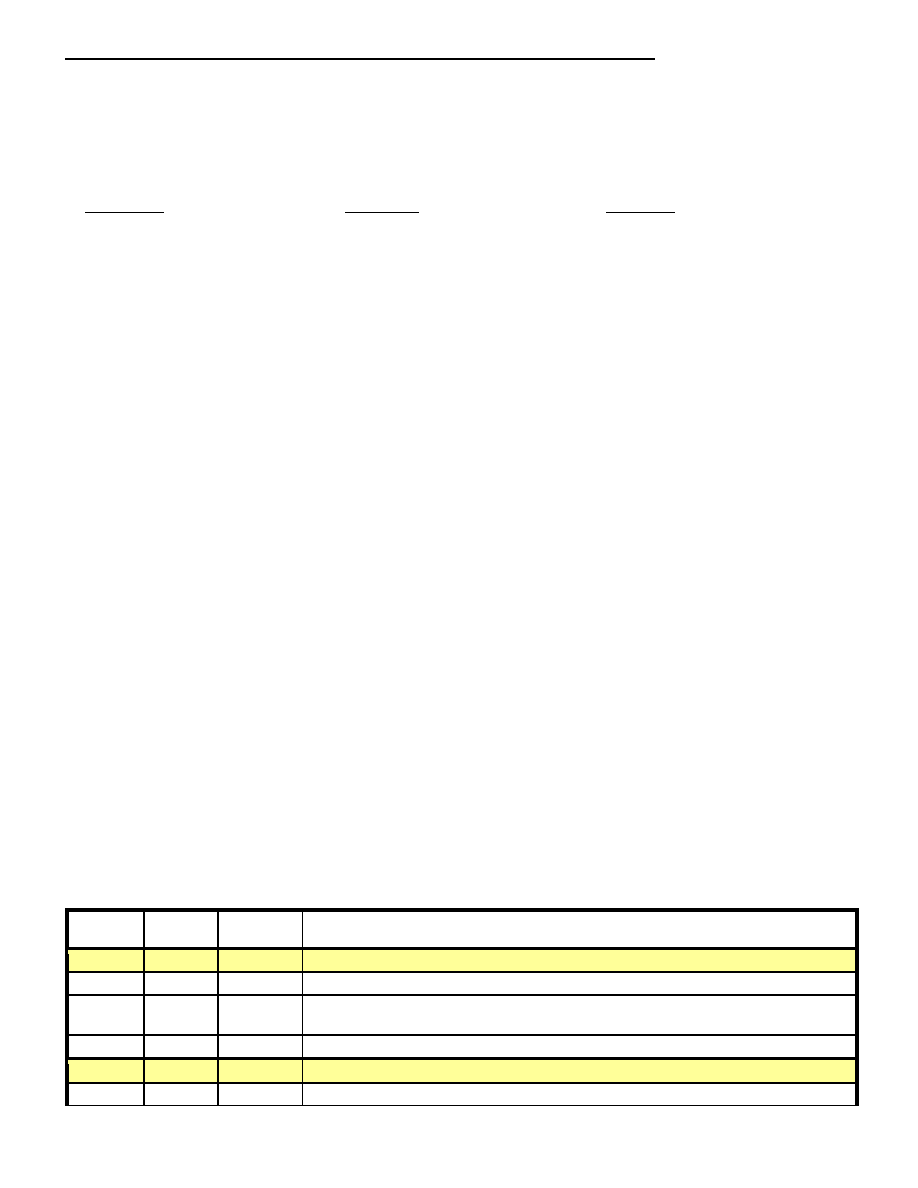
Table 10-3. Global Configuration Registers
G. Field
Name
Addr (A:)
Bit [x:y] Type
Description
IDR.
A:0000h
ID Register. Default: 00.0J.JJh where J = JTAG ID
ID
[31:20] ros-_-_
ID. Reserved
ID
[19:4] ros-_-_
ID. Same information as the lower 16 bits of JTAG CODE ID portion of the JTAG
ID register. JTAG ID[27:12].
ID
[3:0] ros-_-_
Originial Rev ID. Was not modified to reflect Rev A2 ID. Still reads 4’b0000.
GCR.
A:0004h
Global Configuration Register. Default: 0x00.00.08.00
RSVD
[31:28]
Reserved.
相关PDF资料 |
PDF描述 |
|---|---|
| DS34T102GN+ | IC TDM OVER PACKET 484TEBGA |
| DS3501U+H | IC POT NV 128POS HV 10-USOP |
| DS3502U+ | IC POT DGTL NV 128TAP 10-MSOP |
| DS3503U+ | IC POT DGTL NV 128TAP 10-MSOP |
| DS3897MX | IC TXRX BTL TRAPEZIODAL 20-SOIC |
相关代理商/技术参数 |
参数描述 |
|---|---|
| DS34S132GN+ | 功能描述:通信集成电路 - 若干 32Port TDM-Over-Pack Transport Device RoHS:否 制造商:Maxim Integrated 类型:Transport Devices 封装 / 箱体:TECSBGA-256 数据速率:100 Mbps 电源电压-最大:1.89 V, 3.465 V 电源电压-最小:1.71 V, 3.135 V 电源电流:50 mA, 225 mA 最大工作温度:+ 85 C 最小工作温度:- 40 C 封装:Tube |
| DS34S132GNA2+ | 功能描述:通信集成电路 - 若干 32Port TDM-Over-Pack Transport Device RoHS:否 制造商:Maxim Integrated 类型:Transport Devices 封装 / 箱体:TECSBGA-256 数据速率:100 Mbps 电源电压-最大:1.89 V, 3.465 V 电源电压-最小:1.71 V, 3.135 V 电源电流:50 mA, 225 mA 最大工作温度:+ 85 C 最小工作温度:- 40 C 封装:Tube |
| DS34T101 | 制造商:MAXIM 制造商全称:Maxim Integrated Products 功能描述:Single/Dual/Quad/Octal TDM-over-Packet Chip |
| DS34T101_08 | 制造商:MAXIM 制造商全称:Maxim Integrated Products 功能描述:Single/Dual/Quad/Octal TDM-over-Packet Chip |
| DS34T101_09 | 制造商:MAXIM 制造商全称:Maxim Integrated Products 功能描述:Single/Dual/Quad/Octal TDM-over-Packet Chip |
发布紧急采购,3分钟左右您将得到回复。