- 您现在的位置:买卖IC网 > PDF目录1916 > DS34S132GN+ (Maxim Integrated Products)IC TDM OVER PACKET 676-BGA PDF资料下载
参数资料
| 型号: | DS34S132GN+ |
| 厂商: | Maxim Integrated Products |
| 文件页数: | 20/194页 |
| 文件大小: | 0K |
| 描述: | IC TDM OVER PACKET 676-BGA |
| 产品培训模块: | Lead (SnPb) Finish for COTS Obsolescence Mitigation Program |
| 标准包装: | 40 |
| 功能: | TDM-over-Packet(TDMoP) |
| 接口: | TDMoP |
| 电路数: | 1 |
| 电源电压: | 1.8V, 3.3V |
| 工作温度: | -40°C ~ 85°C |
| 安装类型: | 表面贴装 |
| 封装/外壳: | 676-BGA |
| 供应商设备封装: | 676-PBGA(27x27) |
| 包装: | 管件 |
| 其它名称: | 90-34S13+2N0 |
第1页第2页第3页第4页第5页第6页第7页第8页第9页第10页第11页第12页第13页第14页第15页第16页第17页第18页第19页当前第20页第21页第22页第23页第24页第25页第26页第27页第28页第29页第30页第31页第32页第33页第34页第35页第36页第37页第38页第39页第40页第41页第42页第43页第44页第45页第46页第47页第48页第49页第50页第51页第52页第53页第54页第55页第56页第57页第58页第59页第60页第61页第62页第63页第64页第65页第66页第67页第68页第69页第70页第71页第72页第73页第74页第75页第76页第77页第78页第79页第80页第81页第82页第83页第84页第85页第86页第87页第88页第89页第90页第91页第92页第93页第94页第95页第96页第97页第98页第99页第100页第101页第102页第103页第104页第105页第106页第107页第108页第109页第110页第111页第112页第113页第114页第115页第116页第117页第118页第119页第120页第121页第122页第123页第124页第125页第126页第127页第128页第129页第130页第131页第132页第133页第134页第135页第136页第137页第138页第139页第140页第141页第142页第143页第144页第145页第146页第147页第148页第149页第150页第151页第152页第153页第154页第155页第156页第157页第158页第159页第160页第161页第162页第163页第164页第165页第166页第167页第168页第169页第170页第171页第172页第173页第174页第175页第176页第177页第178页第179页第180页第181页第182页第183页第184页第185页第186页第187页第188页第189页第190页第191页第192页第193页第194页
DS34S132 DATA SHEET
19-4750; Rev 1; 07/11
116 of 194
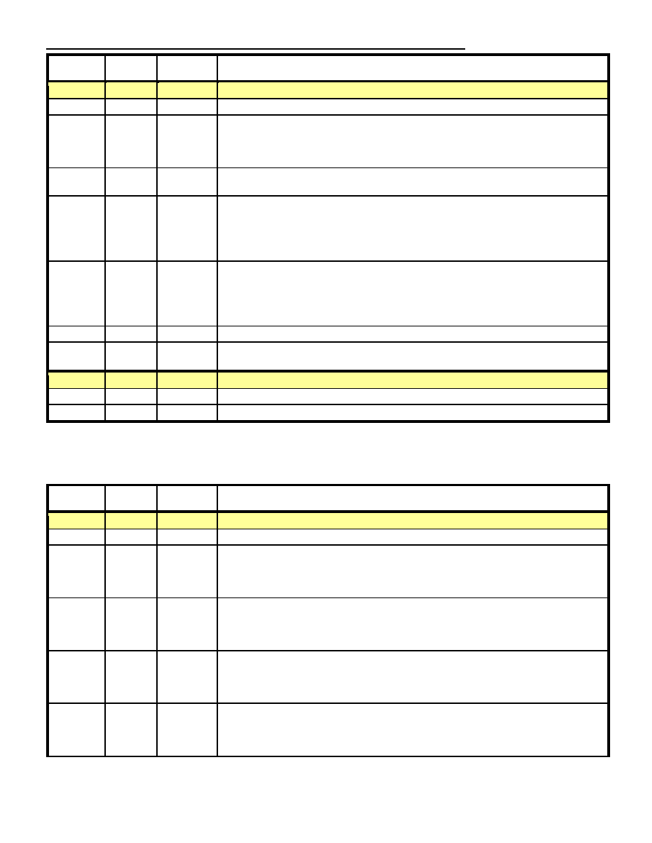
EMI. Field
Name
Addr (A:)
Bit [x:y] Type
Description
DCR2.
A:0394h
DDR SDRAM Configuration Register 2. Default: 00.02.90.10h
RSVD
[31:19]
Reserved.
TRFC
[18:14] rwc-_-_
Time Refresh From Clock selects the time the S132 allows for each SDRAM
refresh cycle to complete. This can be set to any value between the minimum tRFC
allowed by the SDRAM and the max value (0x1F = 248 ns; 0 and 1 are invalid).
Refresh Time = TRFC * 1/freqDDRCLK = TRFC * 8 ns
DCL
[13:11] rwc-_-_
DDR SDRAM CAS Latency specifies the SDRAM CAS Latency.
2 = CAS Latency 2 (all other values are reserved).
DCW
[10:9] rwc-_-_
DDR SDRAM Column Width specifies the external SDRAM Column Width.
0 = 2048 columns per row
1 = 1024 columns per row
2 = 512 columns per row
3 = reserved
DMS
[8:7] rwc-_-_
DDR SDRAM Memory Size specifies the total external SDRAM memory size.
0 = 1 Gbit (two 32 Meg x 16-bit SDRAM devices)
1 = 512 Mbit (one 32 Meg x 16-bit SDRAM device)
2 = 256 Mbit (one 16 Meg x 16-bit SDRAM device)
3 = 128 Mbit (one 8 Meg x 16-bit SDRAM device)
DDW
[6:5] rwc-_-_
Reserved.
DRRS
[4:0] rwc-_-_
DDR SDRAM Refresh Rate Select = time period between each SDRAM Refresh
(SDRAM tREFI parameter) = DRRS * 512ns
DCR3.
A:0398h
DDR SDRAM Configuration Register 3. Default: 00.22.40.00h
DBMR
[31:16] rwc-_-_
Reserved.
DEMR
[15:0] rwc-_-_
Reserved.
10.3.5.2 External Memory Interface Status Registers (EMI.)
Table 10-18. External Memory Interface Status Registers (EMI.)
EMI. Field
Name
Addr (A:)
Bit [x:y] Type
Description
BMSRL.
A:03A0h
Buffer Manager Status Register Latch. Default: 0x00.00.00.00
RSVD
[31:9]
Reserved.
CERCSL
[8] rls-crw-i3
CPU to Ethernet Read Check Status Latch = “1” indicates one or more SDRAM
Read operations were invalid due to EMI.BMCR3.PTSO. The TXP CPU Queue
overlaps with another SDRAM queue due to an invalid EMI Start Address setting.
The combination of CERCSL = 1 and CERCIE = 1 forces G.GSR1.EMIS = 1.
CEWCSL
[7] rls-crw-i3
CPU to Ethernet Write Check Status Latch = “1” indicates one or more SDRAM
Write operations were invalid due to EMI.BMCR3.PTSO. The TXP CPU Queue
overlaps with another SDRAM queue due to an invalid EMI Start Address setting.
The combination of CEWCSL = 1 and CEWCIE = 1 forces G.GSR1.EMIS = 1.
ECRCSL
[6] rls-crw-i3
Ethernet to CPU Read Check Status Latch = “1” indicates one or more SDRAM
Read operations were invalid due to EMI.BMCR3.PRSO. The RXP CPU Queue
overlaps with another SDRAM queue due to an invalid EMI Start Address setting.
The combination of ECRCSL = 1 and ECRCIE = 1 forces G.GSR1.EMIS = 1.
ECWCSL
[5] rls-crw-i3
Ethernet to CPU Write Check Status Latch = “1” indicates one or more SDRAM
Write operations were invalid due to EMI.BMCR3.PRSO. The RXP CPU Queue
overlaps with another SDRAM queue due to an invalid EMI Start Address setting.
The combination of ECWCSL = 1 and ECWCIE = 1 forces G.GSR1.EMIS = 1.
相关PDF资料 |
PDF描述 |
|---|---|
| DS34T102GN+ | IC TDM OVER PACKET 484TEBGA |
| DS3501U+H | IC POT NV 128POS HV 10-USOP |
| DS3502U+ | IC POT DGTL NV 128TAP 10-MSOP |
| DS3503U+ | IC POT DGTL NV 128TAP 10-MSOP |
| DS3897MX | IC TXRX BTL TRAPEZIODAL 20-SOIC |
相关代理商/技术参数 |
参数描述 |
|---|---|
| DS34S132GN+ | 功能描述:通信集成电路 - 若干 32Port TDM-Over-Pack Transport Device RoHS:否 制造商:Maxim Integrated 类型:Transport Devices 封装 / 箱体:TECSBGA-256 数据速率:100 Mbps 电源电压-最大:1.89 V, 3.465 V 电源电压-最小:1.71 V, 3.135 V 电源电流:50 mA, 225 mA 最大工作温度:+ 85 C 最小工作温度:- 40 C 封装:Tube |
| DS34S132GNA2+ | 功能描述:通信集成电路 - 若干 32Port TDM-Over-Pack Transport Device RoHS:否 制造商:Maxim Integrated 类型:Transport Devices 封装 / 箱体:TECSBGA-256 数据速率:100 Mbps 电源电压-最大:1.89 V, 3.465 V 电源电压-最小:1.71 V, 3.135 V 电源电流:50 mA, 225 mA 最大工作温度:+ 85 C 最小工作温度:- 40 C 封装:Tube |
| DS34T101 | 制造商:MAXIM 制造商全称:Maxim Integrated Products 功能描述:Single/Dual/Quad/Octal TDM-over-Packet Chip |
| DS34T101_08 | 制造商:MAXIM 制造商全称:Maxim Integrated Products 功能描述:Single/Dual/Quad/Octal TDM-over-Packet Chip |
| DS34T101_09 | 制造商:MAXIM 制造商全称:Maxim Integrated Products 功能描述:Single/Dual/Quad/Octal TDM-over-Packet Chip |
发布紧急采购,3分钟左右您将得到回复。