- 您现在的位置:买卖IC网 > PDF目录1916 > DS34S132GN+ (Maxim Integrated Products)IC TDM OVER PACKET 676-BGA PDF资料下载
参数资料
| 型号: | DS34S132GN+ |
| 厂商: | Maxim Integrated Products |
| 文件页数: | 138/194页 |
| 文件大小: | 0K |
| 描述: | IC TDM OVER PACKET 676-BGA |
| 产品培训模块: | Lead (SnPb) Finish for COTS Obsolescence Mitigation Program |
| 标准包装: | 40 |
| 功能: | TDM-over-Packet(TDMoP) |
| 接口: | TDMoP |
| 电路数: | 1 |
| 电源电压: | 1.8V, 3.3V |
| 工作温度: | -40°C ~ 85°C |
| 安装类型: | 表面贴装 |
| 封装/外壳: | 676-BGA |
| 供应商设备封装: | 676-PBGA(27x27) |
| 包装: | 管件 |
| 其它名称: | 90-34S13+2N0 |
第1页第2页第3页第4页第5页第6页第7页第8页第9页第10页第11页第12页第13页第14页第15页第16页第17页第18页第19页第20页第21页第22页第23页第24页第25页第26页第27页第28页第29页第30页第31页第32页第33页第34页第35页第36页第37页第38页第39页第40页第41页第42页第43页第44页第45页第46页第47页第48页第49页第50页第51页第52页第53页第54页第55页第56页第57页第58页第59页第60页第61页第62页第63页第64页第65页第66页第67页第68页第69页第70页第71页第72页第73页第74页第75页第76页第77页第78页第79页第80页第81页第82页第83页第84页第85页第86页第87页第88页第89页第90页第91页第92页第93页第94页第95页第96页第97页第98页第99页第100页第101页第102页第103页第104页第105页第106页第107页第108页第109页第110页第111页第112页第113页第114页第115页第116页第117页第118页第119页第120页第121页第122页第123页第124页第125页第126页第127页第128页第129页第130页第131页第132页第133页第134页第135页第136页第137页当前第138页第139页第140页第141页第142页第143页第144页第145页第146页第147页第148页第149页第150页第151页第152页第153页第154页第155页第156页第157页第158页第159页第160页第161页第162页第163页第164页第165页第166页第167页第168页第169页第170页第171页第172页第173页第174页第175页第176页第177页第178页第179页第180页第181页第182页第183页第184页第185页第186页第187页第188页第189页第190页第191页第192页第193页第194页
DS34S132 DATA SHEET
19-4750; Rev 1; 07/11
48 of 194
The PDVT setting specifies how much data must be stored by the Jitter Buffer before “play-out” (FIFO read) begins.
After “play-out” begins the Jitter Buffer will continue to supply data until the Jitter Buffer is empty. If the Jitter Buffer
empties, then the Jitter Buffer must again fill to the PDVT level before data will again be forwarded.
The MJBS watermark can be used to indicate when the level of stored data exceeds an “expected” maximum
(overrun) level. This can be used to monitor for “unexpected” fill levels (e.g. too much data accumulated because of
improperly configured input or output clocks or if the MJBS setting does not allow for the maximum PDV). MJBS
can be monitored to implement a discard process that prevents each Bundle’s Jitter Buffer from over-filling and
adding to the latency of the data (some Clock Recovery Engine firmware revisions may include a function to
discard Jitter Buffer data when MJBS indicates the Jitter Buffer has too much data). The MJBS register should be
programmed to a level that is lower than the JBMD level so that an MJBS Overrun condition can be detected before
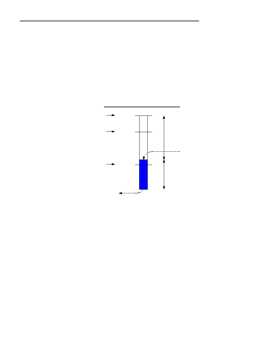
JBMD discarding begins. Figure 9-16 depicts the relationship between the JBMD, MJBS and PDVT settings (the
blue area depicts data that is stored in the Jitter Buffer FIFO).
Figure 9-16. Bundle Jitter Buffer FIFO
MJBS
PDVT
JBMD
This area is empty and
can store SAT/CES TDM
Data from RXP packets.
This area is filled with
SAT/CES TDM Data that
is waiting to be transmited
on the TDM line.
If the SAT/CES TDM Data exceeds the
MJBS Watermark, a Jitter Buffer
Overrun event is counted
(B.BDSR2.JEBEC).
SAT/CES TDM Data is not forwarded to
the TDM Line until the fill level exceeds
the PDVT Watermark.
If the SAT/CES TDM Data exceeds the
JBMD level data, new data is discarded.
Bundle Jitter Buffer FIFO
New SAT/CES packet data is stored here
SAT/CES data is read out from here and sent to TDM Port
The purpose of the Jitter Buffer is to store data that can be transmitted during time periods when the S132 must
wait for a packet that has been “delayed”. At the receiving end of a PW, when a packet is received the PW end
point cannot know whether the PDV for that packet was “zero”, the maximum PDV value or any value in between.
If the receiving PW end point knew that the PDV for a received packet was zero, then the best situation would be to
begin storing data and not forward that data until a time period equal to the maximum PDV. Or, if the PW end point
instead knew that a packet was received with the maximum PDV, then the best situation would be to immediately
forward the data (data will never come later than the maximum PDV; storing would add unnecessary delay).
However the PW end point does not know the PDV level for each packet and thereby must make an assumption.
There are three approaches for setting the PDVT and MJBS values. Each system should be analyzed to determine
which approach is preferred. In each of these approaches the minimum Jitter Buffer delay is equal to the PDVT
setting, while the maximum Jitter Buffer delay (maximum fill level) is either equal to the MJBS or JBMD setting
(MJBS is the maximum if MJBS is monitored as a watermark for discarding; otherwise the maximum is JBMD).
The first approach assumes that it is important to never discard data. This approach results in “2 * Total PDV” ≤
“Jitter Buffer Delay” ≤ “MJBS or JBMD”. This may be the most commonly used setting for existing/installed TDM
over PW services. The settings for this approach are specified by the following equations:
PDVT1 (in ms) = 2 * Total PDV (in ms)
MJBS1 (in ms) = PCT (in ms) + 2 * Total PDV (in ms)
The PCT value is included as part of the MJBS setting to provide a watermark condition that is slightly higher than
the PDVT (playout) watermark and because the originating and terminating ends of the PW cannot be perfectly
phase synchronized together. When the PCT is included as part of the MJBS value, in most cases, the S132 fixed
circuit processing delays can be disregarded (included as part of the PCT value, e.g. BFD PDV).
The second approach assumes that delay must be minimized and only a small amount of discarding should be
allowed. This approach results in a temporary, maximum latency = “2 PDV + PCT”. But as the PDV varies from its
相关PDF资料 |
PDF描述 |
|---|---|
| DS34T102GN+ | IC TDM OVER PACKET 484TEBGA |
| DS3501U+H | IC POT NV 128POS HV 10-USOP |
| DS3502U+ | IC POT DGTL NV 128TAP 10-MSOP |
| DS3503U+ | IC POT DGTL NV 128TAP 10-MSOP |
| DS3897MX | IC TXRX BTL TRAPEZIODAL 20-SOIC |
相关代理商/技术参数 |
参数描述 |
|---|---|
| DS34S132GN+ | 功能描述:通信集成电路 - 若干 32Port TDM-Over-Pack Transport Device RoHS:否 制造商:Maxim Integrated 类型:Transport Devices 封装 / 箱体:TECSBGA-256 数据速率:100 Mbps 电源电压-最大:1.89 V, 3.465 V 电源电压-最小:1.71 V, 3.135 V 电源电流:50 mA, 225 mA 最大工作温度:+ 85 C 最小工作温度:- 40 C 封装:Tube |
| DS34S132GNA2+ | 功能描述:通信集成电路 - 若干 32Port TDM-Over-Pack Transport Device RoHS:否 制造商:Maxim Integrated 类型:Transport Devices 封装 / 箱体:TECSBGA-256 数据速率:100 Mbps 电源电压-最大:1.89 V, 3.465 V 电源电压-最小:1.71 V, 3.135 V 电源电流:50 mA, 225 mA 最大工作温度:+ 85 C 最小工作温度:- 40 C 封装:Tube |
| DS34T101 | 制造商:MAXIM 制造商全称:Maxim Integrated Products 功能描述:Single/Dual/Quad/Octal TDM-over-Packet Chip |
| DS34T101_08 | 制造商:MAXIM 制造商全称:Maxim Integrated Products 功能描述:Single/Dual/Quad/Octal TDM-over-Packet Chip |
| DS34T101_09 | 制造商:MAXIM 制造商全称:Maxim Integrated Products 功能描述:Single/Dual/Quad/Octal TDM-over-Packet Chip |
发布紧急采购,3分钟左右您将得到回复。