- 您现在的位置:买卖IC网 > PDF目录98071 > S5933QE (APPLIEDMICRO INC) PCI BUS CONTROLLER, PQFP160 PDF资料下载
参数资料
| 型号: | S5933QE |
| 厂商: | APPLIEDMICRO INC |
| 元件分类: | 总线控制器 |
| 英文描述: | PCI BUS CONTROLLER, PQFP160 |
| 封装: | PLASTIC, QFP-160 |
| 文件页数: | 132/176页 |
| 文件大小: | 823K |
| 代理商: | S5933QE |
第1页第2页第3页第4页第5页第6页第7页第8页第9页第10页第11页第12页第13页第14页第15页第16页第17页第18页第19页第20页第21页第22页第23页第24页第25页第26页第27页第28页第29页第30页第31页第32页第33页第34页第35页第36页第37页第38页第39页第40页第41页第42页第43页第44页第45页第46页第47页第48页第49页第50页第51页第52页第53页第54页第55页第56页第57页第58页第59页第60页第61页第62页第63页第64页第65页第66页第67页第68页第69页第70页第71页第72页第73页第74页第75页第76页第77页第78页第79页第80页第81页第82页第83页第84页第85页第86页第87页第88页第89页第90页第91页第92页第93页第94页第95页第96页第97页第98页第99页第100页第101页第102页第103页第104页第105页第106页第107页第108页第109页第110页第111页第112页第113页第114页第115页第116页第117页第118页第119页第120页第121页第122页第123页第124页第125页第126页第127页第128页第129页第130页第131页当前第132页第133页第134页第135页第136页第137页第138页第139页第140页第141页第142页第143页第144页第145页第146页第147页第148页第149页第150页第151页第152页第153页第154页第155页第156页第157页第158页第159页第160页第161页第162页第163页第164页第165页第166页第167页第168页第169页第170页第171页第172页第173页第174页第175页第176页
3-69
ADD-ON BUS OPERATION REGISTERS
S5933
ADD-ON CONTROLLED BUS MASTER
WRITE ADDRESS REGISTER (MWAR)
Register Name:
Master Write Address
Add-On Address Offset: 24h
Power-up value:
00000000h
Attribute:
Read/Write
Size:
32 bits
This register is only accessible when Add-On initiated
bus mastering is enabled.
This register is used to establish the PCI address for
data moving from the Add-On bus to the PCI bus
during PCI bus memory write operations. It consists
of a 30-bit counter with the low-order two bits
hardwired as zeros. Transfers may be any non-zero
byte length as defined by the transfer count register,
MWTC and must begin on a DWORD boundary. This
DWORD boundary starting constraint is placed upon
this controller’s PCI bus master transfers so that byte
lane alignment can be maintained between the
S5933 controller’s internal FIFO data path, the Add-
On interface, and the PCI bus.
Note: Applications which require a non-DWORD
starting boundary will need to move the first few
bytes under software program control (and without
using the FIFO) to establish a DWORD boundary.
After the DWORD boundary is established the S5933
can begin the task of PCI bus master data transfers.
The Master Write Address Register is continually up-
dated during the transfer process and will always be
pointing to the next unwritten location. Reading of
this register during a transfer process (done when the
S5933 controller is functioning as a target, i.e. not a
bus master) is permitted and may be used to monitor
the progress of the transfer. During the address
phase for bus master write transfers, the two least
significant bits presented on the PCI bus pins
AD[31:0] will always be zero. This identifies to the
target memory that the burst address sequence will
be in a linear order rather than in an Intel 486 or
Pentium cache line fill sequence. Also, the PCI bus
address bit A1 will always be zero when this control-
ler is the bus master. This signifies to the target that
the S5933 controller is burst capable and that the
target should not arbitrarily disconnect after the first
data phase of this operation.
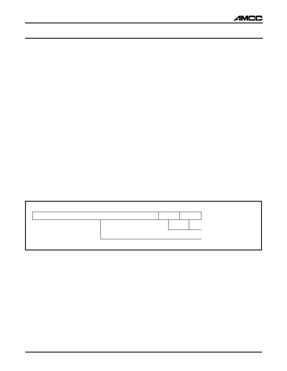
31
0
1
0
2
Bit
Value
DWORD Address (RO)
Write Transfer Address (R/W)
Figure 1. Add-On Controlled Bus Master Write Address Register
相关PDF资料 |
PDF描述 |
|---|---|
| S6A0032 | 16 X 80 DOTS DOT MAT LCD DRVR AND DSPL CTLR, UUC138 |
| S6A0069 | 16 X 40 DOTS DOT MAT LCD DRVR AND DSPL CTLR, UUC80 |
| S6A0078 | 34 X 120 DOTS DOT MAT LCD DRVR AND DSPL CTLR, UUC183 |
| S80296SA40 | 16-BIT, 40 MHz, MICROCONTROLLER, PQFP100 |
| S80486-DX4-75-S-V-8-B | 32-BIT, 75 MHz, MICROPROCESSOR, PQFP208 |
相关代理商/技术参数 |
参数描述 |
|---|---|
| S5935 | 制造商:AMCC 制造商全称:Applied Micro Circuits Corporation 功能描述:PCI Product |
| S5935_07 | 制造商:AMCC 制造商全称:Applied Micro Circuits Corporation 功能描述:PCI Product |
| S59355QRC | 制造商:AppliedMicro 功能描述: |
| S5935QF | 制造商:AMCC 制造商全称:Applied Micro Circuits Corporation 功能描述:PCI Product |
| S5935QRC | 制造商:AppliedMicro 功能描述:PCI Master Device 160-Pin PQFP |
发布紧急采购,3分钟左右您将得到回复。