- 您现在的位置:买卖IC网 > PDF目录98071 > S5933QE (APPLIEDMICRO INC) PCI BUS CONTROLLER, PQFP160 PDF资料下载
参数资料
| 型号: | S5933QE |
| 厂商: | APPLIEDMICRO INC |
| 元件分类: | 总线控制器 |
| 英文描述: | PCI BUS CONTROLLER, PQFP160 |
| 封装: | PLASTIC, QFP-160 |
| 文件页数: | 15/176页 |
| 文件大小: | 823K |
| 代理商: | S5933QE |
第1页第2页第3页第4页第5页第6页第7页第8页第9页第10页第11页第12页第13页第14页当前第15页第16页第17页第18页第19页第20页第21页第22页第23页第24页第25页第26页第27页第28页第29页第30页第31页第32页第33页第34页第35页第36页第37页第38页第39页第40页第41页第42页第43页第44页第45页第46页第47页第48页第49页第50页第51页第52页第53页第54页第55页第56页第57页第58页第59页第60页第61页第62页第63页第64页第65页第66页第67页第68页第69页第70页第71页第72页第73页第74页第75页第76页第77页第78页第79页第80页第81页第82页第83页第84页第85页第86页第87页第88页第89页第90页第91页第92页第93页第94页第95页第96页第97页第98页第99页第100页第101页第102页第103页第104页第105页第106页第107页第108页第109页第110页第111页第112页第113页第114页第115页第116页第117页第118页第119页第120页第121页第122页第123页第124页第125页第126页第127页第128页第129页第130页第131页第132页第133页第134页第135页第136页第137页第138页第139页第140页第141页第142页第143页第144页第145页第146页第147页第148页第149页第150页第151页第152页第153页第154页第155页第156页第157页第158页第159页第160页第161页第162页第163页第164页第165页第166页第167页第168页第169页第170页第171页第172页第173页第174页第175页第176页
3-124
FIFO OVERVIEW
S5933
The configurable FIFO advance condition may be
used to transfer data to and from Add-On interfaces
which are not 32-bits wide. For a 16-bit Add-On bus,
the Add-On to PCI FIFO advance condition can be
set to byte 2. This allows a 16-bit write to the lower 16-
bits of the FIFO register (bytes 0 and 1) and a second
write to the upper 16-bits of the FIFO register (bytes
2 and 3). The FIFO does not advance until the
second access. This allows the Add-On to operate
with 16-bit data, while the PCI bus maintains a 32-bit
data path.
Notes:
1. During operation, the INTCSR FIFO advance condition bits
(D29:26) should only be changed when the FIFO is empty and
is idle on both the Add-On and PCI interfaces.
Endian Conversion
Bits D31:30 and D25:24 of the INTCSR PCI Opera-
tion Register control endian conversion operations for
the FIFO (Figure 1). When endian conversion is per-
formed, it affects data passing in either direction
through the FIFO interface. Figures 2a and 2b show
16-bit and 32-bit endian conversion. It is important to
note that endian conversion is performed on data BE-
FORE it enters the FIFO. This affects the FIFO ad-
vance condition. Example: the FIFO is configured to
perform 32-bit endian conversion on data, and the
FIFO advance condition is set to byte 0. Byte 3 is
written into the FIFO (BE3# asserted). After the
endian conversion, byte 3 becomes byte 0, and the
FIFO advances. This behavior must be considered
when not performing full 32-bit accesses to the FIFO.
Notes:
1. During operation, the INTCSR FIFO endian conversion bits
(D25:24) and 64-bit access bits (D31:30) should only be
changed when the FIFO is empty and is idle on both the Add-
On and PCI interfaces.
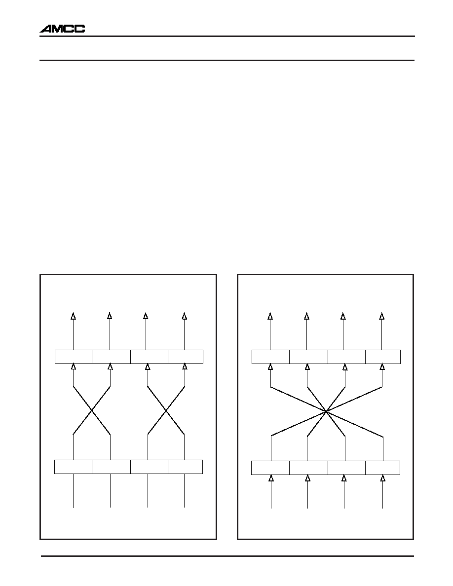
Figure 2a. 16-bit Endian Conversion
DESTINATION
D 31-24
D 23-16
D 15-8
D 7-0
BYTE 3
BYTE 2
BYTE 1
BYTE 0
BYTE 3
BYTE 2
BYTE 1
BYTE 0
D 31-24
D 23-16
D 15-8
D 7-0
SOURCE
Figure 2b. 32-bit Endian Conversion
DESTINATION
D 31-24
D 23-16
D 15-8
D 7-0
BYTE 3
BYTE 2
BYTE 1
BYTE 0
BYTE 3
BYTE 2
BYTE 1
BYTE 0
D 31-24
D 23-16
D 15-8
D 7-0
SOURCE
相关PDF资料 |
PDF描述 |
|---|---|
| S6A0032 | 16 X 80 DOTS DOT MAT LCD DRVR AND DSPL CTLR, UUC138 |
| S6A0069 | 16 X 40 DOTS DOT MAT LCD DRVR AND DSPL CTLR, UUC80 |
| S6A0078 | 34 X 120 DOTS DOT MAT LCD DRVR AND DSPL CTLR, UUC183 |
| S80296SA40 | 16-BIT, 40 MHz, MICROCONTROLLER, PQFP100 |
| S80486-DX4-75-S-V-8-B | 32-BIT, 75 MHz, MICROPROCESSOR, PQFP208 |
相关代理商/技术参数 |
参数描述 |
|---|---|
| S5935 | 制造商:AMCC 制造商全称:Applied Micro Circuits Corporation 功能描述:PCI Product |
| S5935_07 | 制造商:AMCC 制造商全称:Applied Micro Circuits Corporation 功能描述:PCI Product |
| S59355QRC | 制造商:AppliedMicro 功能描述: |
| S5935QF | 制造商:AMCC 制造商全称:Applied Micro Circuits Corporation 功能描述:PCI Product |
| S5935QRC | 制造商:AppliedMicro 功能描述:PCI Master Device 160-Pin PQFP |
发布紧急采购,3分钟左右您将得到回复。