- 您现在的位置:买卖IC网 > PDF目录98071 > S5933QE (APPLIEDMICRO INC) PCI BUS CONTROLLER, PQFP160 PDF资料下载
参数资料
| 型号: | S5933QE |
| 厂商: | APPLIEDMICRO INC |
| 元件分类: | 总线控制器 |
| 英文描述: | PCI BUS CONTROLLER, PQFP160 |
| 封装: | PLASTIC, QFP-160 |
| 文件页数: | 14/176页 |
| 文件大小: | 823K |
| 代理商: | S5933QE |
第1页第2页第3页第4页第5页第6页第7页第8页第9页第10页第11页第12页第13页当前第14页第15页第16页第17页第18页第19页第20页第21页第22页第23页第24页第25页第26页第27页第28页第29页第30页第31页第32页第33页第34页第35页第36页第37页第38页第39页第40页第41页第42页第43页第44页第45页第46页第47页第48页第49页第50页第51页第52页第53页第54页第55页第56页第57页第58页第59页第60页第61页第62页第63页第64页第65页第66页第67页第68页第69页第70页第71页第72页第73页第74页第75页第76页第77页第78页第79页第80页第81页第82页第83页第84页第85页第86页第87页第88页第89页第90页第91页第92页第93页第94页第95页第96页第97页第98页第99页第100页第101页第102页第103页第104页第105页第106页第107页第108页第109页第110页第111页第112页第113页第114页第115页第116页第117页第118页第119页第120页第121页第122页第123页第124页第125页第126页第127页第128页第129页第130页第131页第132页第133页第134页第135页第136页第137页第138页第139页第140页第141页第142页第143页第144页第145页第146页第147页第148页第149页第150页第151页第152页第153页第154页第155页第156页第157页第158页第159页第160页第161页第162页第163页第164页第165页第166页第167页第168页第169页第170页第171页第172页第173页第174页第175页第176页
3-123
FIFO OVERVIEW
S5933
FIFO OVERVIEW
The S5933 has two internal FIFOs. One FIFO is for
PCI bus to Add-On bus, the other FIFO is for Add-On
bus to PCI bus transfers. Each of these has eight 32-
bit registers. The FIFOs are both addressed through
a single PCI/Add-On Operation Register offset, but
which internal FIFO is accessed is determined by
whether the access is a read or write.
The FIFO may be either a PCI target or a PCI initia-
tor. As a target, the FIFO allows a PCI bus master to
access Add-On data. The FIFO also allows the
S5933 to become a PCI initiator. Read and write ad-
dress registers and transfer count registers allow the
S5933 to perform DMA transfers across the PCI bus.
The FIFO may act as initiator and a target at different
times in the same application.
The FIFO can be configured to support various Add-
On bus configurations. FIFO status and control signals
allow simple cascading into an external FIFO, the Add-
On bus can be 8-, 16-, or 32-bits wide, and data
endian conversion is optional to support any type of
Add-On CPU. PCI and Add-On interrupt capabilities
are available to support bus mastering through the
FIFO.
FUNCTIONAL DESCRIPTION
The S5933 FIFO interface allows a high degree of
functionality and flexibility. Different FIFO manage-
ment schemes, endian conversion schemes, and ad-
vance conditions allow for a wide variety of Add-On
interfaces. Applications may implement the FIFO as
either a PCI target or program it to enable the S5933
to be a PCI initiator (bus master). The following sec-
tions describe, on a functional level, the capabilities
of the S5933 FIFO interface.
FIFO Buffer Management and Endian
Conversion
The S5933 provides a high degree of flexibility for
controlling the data flow through the FIFO. Each
FIFO (PCI to Add-On and Add-On to PCI) has a spe-
cific FIFO advance condition. For FIFO writes, the
byte which signifies a location is full is configurable.
For FIFO reads, the byte which signifies a location is
empty is configurable. This ability is useful for trans-
ferring data through the FIFO with Add-Ons which
are not 32-bits wide. Endian conversion may also be
performed on data passing through the FIFO.
FIFO Advance Conditions
The specific byte lane used to advance the FIFO,
when accessed, is determined individually for each
FIFO interface (PCI and Add-On). The control bits to
set the advance condition are D29:26 of the Interrupt
Control/Status Register (INTCSR) in the PCI Opera-
tion Registers (Figure 1). The default FIFO advance
condition is set to byte 0. With the default setting, a
write to the FIFO with BE0# asserted indicates that
the FIFO location is now full, advancing the FIFO
pointer to the next location. BE0# does not have to be
the only byte enable asserted. Note, the FIFO advance
condition may be different for the PCI to Add-On FIFO
and the Add-On to PCI FIFO directions.
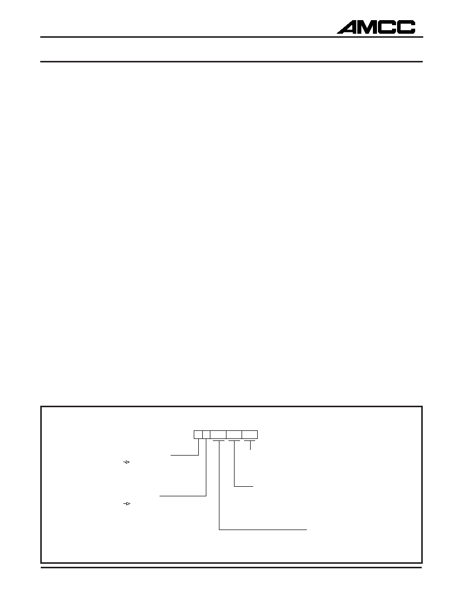
Figure 1. INTCSR FIFO Advance and Endian Control Bits
INTCSR
0
1
0 NO CONVERSION (DEFAULT)
1 16 BIT ENDIAN CONV.
0 32 BIT ENDIAN CONV.
1 64 BIT ENDIAN CONV
FIFO ADVANCE CONTROL
PCI INTERFACE
0 0 BYTE 0 (DEFAULT)
0 1 BYTE 1
1 0 BYTE 2
1 1 BYTE 3
FIFO ADVANCE CONTROL
ADD-ON INTERFACE
0 0 BYTE 0 (DEFAULT)
0 1 BYTE 1
1 0 BYTE 2
1 1 BYTE 3
PCI TO ADD-ON FIFO
PCI
ADD-ON DWORD
TOGGLE
0 = BYTES 0-3 (DEFAULT)
1 = BYTE 4-7 (NOTE1)
ADD-ON TO PCI FIFO
ADD-ON
PCI DWORD
TOGGLE
0 = BYTES 0-3 (DEFAULT)
1 = BYTE 4-7 (NOTE1)
NOTE 1: D24 AND D25 MUST BE ALSO "1"
31 30 29
28 27
26 25
24
相关PDF资料 |
PDF描述 |
|---|---|
| S6A0032 | 16 X 80 DOTS DOT MAT LCD DRVR AND DSPL CTLR, UUC138 |
| S6A0069 | 16 X 40 DOTS DOT MAT LCD DRVR AND DSPL CTLR, UUC80 |
| S6A0078 | 34 X 120 DOTS DOT MAT LCD DRVR AND DSPL CTLR, UUC183 |
| S80296SA40 | 16-BIT, 40 MHz, MICROCONTROLLER, PQFP100 |
| S80486-DX4-75-S-V-8-B | 32-BIT, 75 MHz, MICROPROCESSOR, PQFP208 |
相关代理商/技术参数 |
参数描述 |
|---|---|
| S5935 | 制造商:AMCC 制造商全称:Applied Micro Circuits Corporation 功能描述:PCI Product |
| S5935_07 | 制造商:AMCC 制造商全称:Applied Micro Circuits Corporation 功能描述:PCI Product |
| S59355QRC | 制造商:AppliedMicro 功能描述: |
| S5935QF | 制造商:AMCC 制造商全称:Applied Micro Circuits Corporation 功能描述:PCI Product |
| S5935QRC | 制造商:AppliedMicro 功能描述:PCI Master Device 160-Pin PQFP |
发布紧急采购,3分钟左右您将得到回复。