- 您现在的位置:买卖IC网 > PDF目录98071 > S5933QE (APPLIEDMICRO INC) PCI BUS CONTROLLER, PQFP160 PDF资料下载
参数资料
| 型号: | S5933QE |
| 厂商: | APPLIEDMICRO INC |
| 元件分类: | 总线控制器 |
| 英文描述: | PCI BUS CONTROLLER, PQFP160 |
| 封装: | PLASTIC, QFP-160 |
| 文件页数: | 150/176页 |
| 文件大小: | 823K |
| 代理商: | S5933QE |
第1页第2页第3页第4页第5页第6页第7页第8页第9页第10页第11页第12页第13页第14页第15页第16页第17页第18页第19页第20页第21页第22页第23页第24页第25页第26页第27页第28页第29页第30页第31页第32页第33页第34页第35页第36页第37页第38页第39页第40页第41页第42页第43页第44页第45页第46页第47页第48页第49页第50页第51页第52页第53页第54页第55页第56页第57页第58页第59页第60页第61页第62页第63页第64页第65页第66页第67页第68页第69页第70页第71页第72页第73页第74页第75页第76页第77页第78页第79页第80页第81页第82页第83页第84页第85页第86页第87页第88页第89页第90页第91页第92页第93页第94页第95页第96页第97页第98页第99页第100页第101页第102页第103页第104页第105页第106页第107页第108页第109页第110页第111页第112页第113页第114页第115页第116页第117页第118页第119页第120页第121页第122页第123页第124页第125页第126页第127页第128页第129页第130页第131页第132页第133页第134页第135页第136页第137页第138页第139页第140页第141页第142页第143页第144页第145页第146页第147页第148页第149页当前第150页第151页第152页第153页第154页第155页第156页第157页第158页第159页第160页第161页第162页第163页第164页第165页第166页第167页第168页第169页第170页第171页第172页第173页第174页第175页第176页
3-86
INITIALIZATION
S5933
PCI BUS CONFIGURATION CYCLES
Cycles beginning with the assertion IDSEL and
FRAME# along with the two configuration command
states for C/BE[3:0] (configuration read or write) ac-
cess an individual device’s configuration space. Dur-
ing the address phase of the configuration cycle just
described, the values of AD0 and AD1 identify if the
access is a Type 0 configuration cycle or a Type 1
configuration cycle. Type 0 cycles have AD0 and
AD1 equal to 0 and are used to access PCI bus
agents. Type 1 configuration cycles are intended only
for bridge devices and have AD0 as a 1 with AD1 as
a 0 during the address phase.
The S5933 PCI device is a bus agent (not a bridge)
and responds only to a Type 0 configuration ac-
cesses. Figure 5 depicts the state of the AD bus
during the address phase of a Type 0 configuration
access. The S5933 controller does not support the
multiple function numbers field (AD[10:8]) and only
responds to the all-zero function number value.
The configuration registers for the S5933 PCI control-
ler can only be accessed under the following
conditions:
IDSEL high (PCI slot unique signal which
identifies access to configuration registers)
along with FRAME# low.
Address bits A0 and A1 are 0 (Identifies a Type
0 configuration access).
Address bits A31-A11 are ignored.
Address bits A8, A9, and A10 are 0 (Function
number field of zero supported).
Command bits, C/BE[3:0]# must identify a
configuration cycle command (101X).
Figure 6 describes the signal timing relationships for
configuration read cycles. Figure 7 describes configu-
ration write cycles.
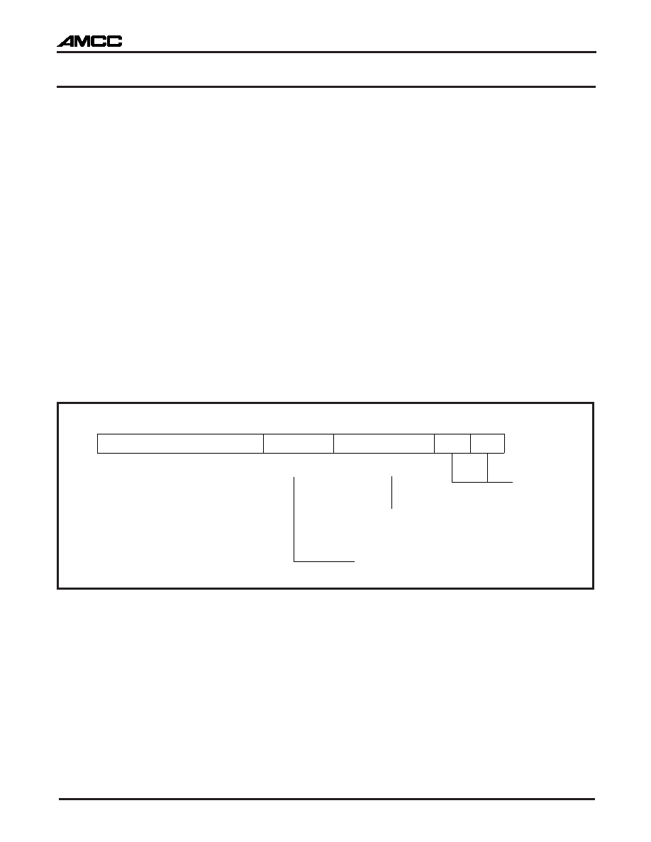
Figure 5. PCI AD Bus Definition During a Type 0 Configuration Access
FUNCTION
NUMBER
RESERVED
REGISTER
NUMBER
00
31
11
10
8
7
2
1
0
TYPE 0
00XXXXXX
-
INTERNAL REGISTER
ADDRESS
(DEVICE ID, ETC.)
ONLY 000 VALUE SUPPORTED BY THIS
DEVICE.
相关PDF资料 |
PDF描述 |
|---|---|
| S6A0032 | 16 X 80 DOTS DOT MAT LCD DRVR AND DSPL CTLR, UUC138 |
| S6A0069 | 16 X 40 DOTS DOT MAT LCD DRVR AND DSPL CTLR, UUC80 |
| S6A0078 | 34 X 120 DOTS DOT MAT LCD DRVR AND DSPL CTLR, UUC183 |
| S80296SA40 | 16-BIT, 40 MHz, MICROCONTROLLER, PQFP100 |
| S80486-DX4-75-S-V-8-B | 32-BIT, 75 MHz, MICROPROCESSOR, PQFP208 |
相关代理商/技术参数 |
参数描述 |
|---|---|
| S5935 | 制造商:AMCC 制造商全称:Applied Micro Circuits Corporation 功能描述:PCI Product |
| S5935_07 | 制造商:AMCC 制造商全称:Applied Micro Circuits Corporation 功能描述:PCI Product |
| S59355QRC | 制造商:AppliedMicro 功能描述: |
| S5935QF | 制造商:AMCC 制造商全称:Applied Micro Circuits Corporation 功能描述:PCI Product |
| S5935QRC | 制造商:AppliedMicro 功能描述:PCI Master Device 160-Pin PQFP |
发布紧急采购,3分钟左右您将得到回复。