- 您现在的位置:买卖IC网 > PDF目录69324 > S1C17554B00E10H 16-BIT, FLASH, 24 MHz, RISC MICROCONTROLLER, PBGA48 PDF资料下载
参数资料
| 型号: | S1C17554B00E10H |
| 元件分类: | 微控制器/微处理器 |
| 英文描述: | 16-BIT, FLASH, 24 MHz, RISC MICROCONTROLLER, PBGA48 |
| 封装: | 3.137 X 3.137 MM, 0.72 MM HEIGHT, 0.40 MM PITCH, WCSP-48 |
| 文件页数: | 245/318页 |
| 文件大小: | 2643K |
| 代理商: | S1C17554B00E10H |
第1页第2页第3页第4页第5页第6页第7页第8页第9页第10页第11页第12页第13页第14页第15页第16页第17页第18页第19页第20页第21页第22页第23页第24页第25页第26页第27页第28页第29页第30页第31页第32页第33页第34页第35页第36页第37页第38页第39页第40页第41页第42页第43页第44页第45页第46页第47页第48页第49页第50页第51页第52页第53页第54页第55页第56页第57页第58页第59页第60页第61页第62页第63页第64页第65页第66页第67页第68页第69页第70页第71页第72页第73页第74页第75页第76页第77页第78页第79页第80页第81页第82页第83页第84页第85页第86页第87页第88页第89页第90页第91页第92页第93页第94页第95页第96页第97页第98页第99页第100页第101页第102页第103页第104页第105页第106页第107页第108页第109页第110页第111页第112页第113页第114页第115页第116页第117页第118页第119页第120页第121页第122页第123页第124页第125页第126页第127页第128页第129页第130页第131页第132页第133页第134页第135页第136页第137页第138页第139页第140页第141页第142页第143页第144页第145页第146页第147页第148页第149页第150页第151页第152页第153页第154页第155页第156页第157页第158页第159页第160页第161页第162页第163页第164页第165页第166页第167页第168页第169页第170页第171页第172页第173页第174页第175页第176页第177页第178页第179页第180页第181页第182页第183页第184页第185页第186页第187页第188页第189页第190页第191页第192页第193页第194页第195页第196页第197页第198页第199页第200页第201页第202页第203页第204页第205页第206页第207页第208页第209页第210页第211页第212页第213页第214页第215页第216页第217页第218页第219页第220页第221页第222页第223页第224页第225页第226页第227页第228页第229页第230页第231页第232页第233页第234页第235页第236页第237页第238页第239页第240页第241页第242页第243页第244页当前第245页第246页第247页第248页第249页第250页第251页第252页第253页第254页第255页第256页第257页第258页第259页第260页第261页第262页第263页第264页第265页第266页第267页第268页第269页第270页第271页第272页第273页第274页第275页第276页第277页第278页第279页第280页第281页第282页第283页第284页第285页第286页第287页第288页第289页第290页第291页第292页第293页第294页第295页第296页第297页第298页第299页第300页第301页第302页第303页第304页第305页第306页第307页第308页第309页第310页第311页第312页第313页第314页第315页第316页第317页第318页
3 MEMORY MAP, BUS CONTROL
S1C17554/564 TECHNICAL MANUAL
Seiko Epson Corporation
3-1
Memory Map, Bus Control
3
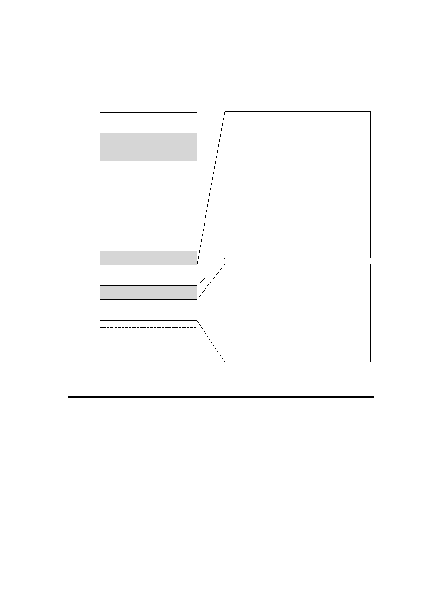
Figure 3.1 shows the S1C17554/564 memory map.
Flash area
(128K bytes)
(Device size: 16 bits)
Vector table
Internal peripheral area 2
(4K bytes)
Internal peripheral area 1
(1K bytes)
Reserved for core I/O area
(1K bytes)
reserved
0xff ffff
0xff fc00
0xff fbff
0x02 8000
0x02 7fff
0x00 8000
0x00 7fff
0x00 6000
0x00 5fff
0x00 5000
0x00 4fff
0x00 4400
0x00 43ff
0x00 4000
0x00 3fff
0x00 3fc0
0x00 0000
0x43c0–0x43ff
0x4380–0x43bf
0x4360–0x437f
0x4340–0x435f
0x4320–0x433f
0x42e0–0x431f
0x4280–0x42df
0x4220–0x427f
0x4200–0x421f
0x4140–0x41ff
0x4100–0x413f
0x4040–0x40ff
0x4020–0x403f
0x4000–0x401f
reserved
SPI Ch.1–2
I2C slave
I2C master
SPI Ch.0
Interrupt controller
Fine mode 16-bit timer Ch.1
16-bit timer Ch.0–2
Fine mode 16-bit timer Ch.0
reserved
UART Ch.0–1
reserved
MISC registers
reserved
Debug RAM area (64 bytes)
Internal RAM area
(16K bytes)
(Device size: 32 bits)
0x5500–0x5fff
0x5480–0x54ff
0x5400–0x547f
0x53a0–0x53ff
0x5380–0x539f
0x5360–0x537f
0x5340–0x535f
0x5320–0x533f
0x52c0–0x531f
0x52a0–0x52bf
0x5280–0x529f
0x5200–0x527f
0x5140–0x51ff
0x5120–0x513f
0x5100–0x511f
0x50c0–0x50ff
0x50a0–0x50bf
0x5060–0x509f
0x5040–0x505f
0x5020–0x503f
0x5000–0x501f
reserved
Flash controller
16-bit PWM timer Ch.0–3
reserved
A/D converter
reserved
IR remote controller
MISC registers
reserved
Port MUX
reserved
P ports
reserved
Power generator (S1C17564)
reserved
USI Ch.0–1 (S1C17564)
reserved
Clock generator
Watchdog timer
Stopwatch timer
Clock timer
–
(16 bits)
–
(16 bits)
–
(16 bits)
–
(8 bits)
–
(8 bits)
–
(8 bits)
–
(8 bits)
–
(8 bits)
–
(16 bits)
–
(8 bits)
–
(8 bits)
–
Peripheral function
(Device size)
1 S1C17554/564 Memory Map
Figure 3.
Bus Cycle
3.1
The CPU uses the system clock for bus access operations. For more information on the system clock, see “System
Clock Switching” in the “Clock Generator (CLG)” chapter.
Note that the Flash area and other areas require different number of system clocks for one bus cycle as follows:
Instruction/data read from areas other than the Flash area:
One system clock per one bus cycle
Instruction read from the Flash area:
One to three system clocks or equivalent per one bus cycle
Data read from the Flash area:
Two to four system clocks per one bus cycle
Furthermore, the number of bus accesses depends on the CPU instruction (access size) and device size.
相关PDF资料 |
PDF描述 |
|---|---|
| S1C17554B00E10M | 16-BIT, FLASH, 24 MHz, RISC MICROCONTROLLER, PBGA48 |
| S1C17554B00E10P | 16-BIT, FLASH, 24 MHz, RISC MICROCONTROLLER, PBGA48 |
| S1C17554B00E10R | 16-BIT, FLASH, 24 MHz, RISC MICROCONTROLLER, PBGA48 |
| S1C17554D00E10E | 16-BIT, FLASH, 24 MHz, RISC MICROCONTROLLER, UUC |
| S1C17554D00E10F | 16-BIT, FLASH, 24 MHz, RISC MICROCONTROLLER, UUC |
相关代理商/技术参数 |
参数描述 |
|---|---|
| S1C17555 | 制造商:EPSON 制造商全称:EPSON 功能描述:16-bit Single Chip Microcontroller |
| S1C17564 | 制造商:EPSON 制造商全称:EPSON 功能描述:16-bit Single Chip Microcontroller |
| S1C17564D111000 | 制造商:Epson Electronics America Inc 功能描述:16-bit, 128KB Flash (OSC3 = Ceramic) |
| S1C17564F111100 | 功能描述:显示驱动器和控制器 16-bit, 128KB Flash RoHS:否 制造商:Panasonic Electronic Components 工作电源电压:2.7 V to 5.5 V 最大工作温度: 安装风格:SMD/SMT 封装 / 箱体:QFN-44 封装:Reel |
| S1C17565 | 制造商:EPSON 制造商全称:EPSON 功能描述:16-bit Single Chip Microcontroller |
发布紧急采购,3分钟左右您将得到回复。