- 您现在的位置:买卖IC网 > PDF目录45052 > M66596WG UNIVERSAL SERIAL BUS CONTROLLER, PBGA64 PDF资料下载
参数资料
| 型号: | M66596WG |
| 元件分类: | 总线控制器 |
| 英文描述: | UNIVERSAL SERIAL BUS CONTROLLER, PBGA64 |
| 封装: | 0.80 MM PITCH, FBGA-64 |
| 文件页数: | 10/133页 |
| 文件大小: | 1611K |
| 代理商: | M66596WG |
第1页第2页第3页第4页第5页第6页第7页第8页第9页当前第10页第11页第12页第13页第14页第15页第16页第17页第18页第19页第20页第21页第22页第23页第24页第25页第26页第27页第28页第29页第30页第31页第32页第33页第34页第35页第36页第37页第38页第39页第40页第41页第42页第43页第44页第45页第46页第47页第48页第49页第50页第51页第52页第53页第54页第55页第56页第57页第58页第59页第60页第61页第62页第63页第64页第65页第66页第67页第68页第69页第70页第71页第72页第73页第74页第75页第76页第77页第78页第79页第80页第81页第82页第83页第84页第85页第86页第87页第88页第89页第90页第91页第92页第93页第94页第95页第96页第97页第98页第99页第100页第101页第102页第103页第104页第105页第106页第107页第108页第109页第110页第111页第112页第113页第114页第115页第116页第117页第118页第119页第120页第121页第122页第123页第124页第125页第126页第127页第128页第129页第130页第131页第132页第133页
M66596FP/WG
rev .1.00
2006.3.14
page 105 of 127
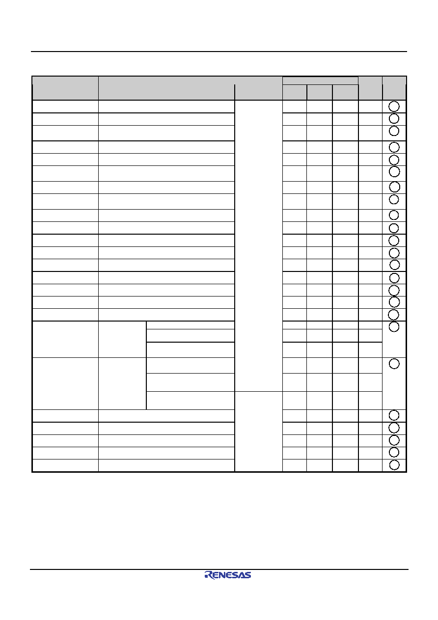
4.8 Required timing conditions (VIF = 2.7~3.6V, or 1.6~2.0V)
Rated value
Symbol
Item
Measurement
conditions /
other
Min.
Typ.
Max.
Unit
Ref.
no.
tsuw (A)
Address write setup time
CL=50 pF
30
ns
30
tsur (A)
Address read setup time
0
ns
31
tsu (A - ALE)
Address setup time when using multiplex
bus
10
ns
32
thw (A)
Address write hold time
0
ns
33
thr (A)
Address read hold time
30
ns
34
th (A - ALE)
Address setup hold time when using
multiplex bus
0
ns
35
tw (ALE)
ALE pulse width when using multiplex bus
10
ns
36
tdwr (ALE - CTRL)
Write / read delay time when using multiplex
bus
7
ns
37
trec (ALE)
ALE recovery time when using multiplex bus
0
ns
38
tw (CTRL)
Control pulse width (write)
30
ns
39
trec (CTRL)
Control recovery time (FIFO)
30
ns
40
trecr (CTRL)
Control recovery time (REG)
12
ns
41
twr (CTRL)
Control pulse width (read)
30
ns
42
tsu (D)
Data setup time
20
ns
43
th (D)
Data hold time
0
ns
44
tsu (Dend)
DEND input setup time
30
ns
45
th (Dend)
DEND input hold time
0
ns
46
8-bit FIFO access
30
ns
16-bit FIFO access
50
ns
tw (cycle)
FIFO access
cycle time
8- / a6-bit FIFO access
when using multiplex bus
84
ns
47
When using split bus, and
Obus=0
12
ns
When using split bus, and
Obus=1
30
ns
tw (CTRL_B)
Control pulse
width when
using burst
transfers
When using DMA transfers
with CPU bus
30
ns
48
trec (CTRL_B)
Control recovery time for burst transfers
12
ns
49
tsud (A)
DMA address write setup time
15
ns
50
thd (A)
DMA address write hold time
0
ns
51
tw (RST)
Reset pulse width time
100
ns
52
tst (RST)
Control starts time after reset
500
ns
53
Key
tsuw: Write setup time, tsur: Read setup time, tsu: Setup time
thw: Write hold time, thr: Read hold time, th: Hold time, tw: Pulse width, twr: Read pulse width
tdwr: Read / write delay time, trec: Recovery time, trecr: Register recovery time
tsud: DMA setup time, thd: DMA hold time, tst: Start time
(A): Address, (D): Data, (CTRL): Control, (CTRL_B): Burst control, (ALE): ALE
*1) Only for data writing, when the DACK0_N signal is assuring an active period of at least 30 ns, the DSTB0_N
signal can be accessed at a minimum of 12 ns.
相关PDF资料 |
PDF描述 |
|---|---|
| M6XXLFXI | OTHER CLOCK GENERATOR, QCC16 |
| M300LFXIT | 50 MHz, OTHER CLOCK GENERATOR, QCC16 |
| M74HC00C1R | HC/UH SERIES, QUAD 2-INPUT NAND GATE, PQCC20 |
| M74HC157B1N | HC/UH SERIES, QUAD 2 LINE TO 1 LINE MULTIPLEXER, TRUE OUTPUT, PDIP16 |
| M74HC158C1 | HC/UH SERIES, QUAD 2 LINE TO 1 LINE MULTIPLEXER, INVERTED OUTPUT, PQCC20 |
相关代理商/技术参数 |
参数描述 |
|---|---|
| M66596WG#RB0Z | 制造商:Renesas Electronics 功能描述:Tray 制造商:Renesas 功能描述:0 |
| M6668 | 制造商:Tamura Corporation of America 功能描述: |
| M66700P | 制造商:MITSUBISHI 制造商全称:Mitsubishi Electric Semiconductor 功能描述:DUAL HIGH-SPEED CCD CLOCK DRIVER |
| M66700WP | 制造商:MITSUBISHI 制造商全称:Mitsubishi Electric Semiconductor 功能描述:DUAL HIGH-SPEED CCD CLOCK DRIVER |
| M66701P | 制造商:MITSUBISHI 制造商全称:Mitsubishi Electric Semiconductor 功能描述:DUAL HIGH-SPEED CCD CLOCK DRIVER |
发布紧急采购,3分钟左右您将得到回复。