- 您现在的位置:买卖IC网 > PDF目录45052 > M66596WG UNIVERSAL SERIAL BUS CONTROLLER, PBGA64 PDF资料下载
参数资料
| 型号: | M66596WG |
| 元件分类: | 总线控制器 |
| 英文描述: | UNIVERSAL SERIAL BUS CONTROLLER, PBGA64 |
| 封装: | 0.80 MM PITCH, FBGA-64 |
| 文件页数: | 58/133页 |
| 文件大小: | 1611K |
| 代理商: | M66596WG |
第1页第2页第3页第4页第5页第6页第7页第8页第9页第10页第11页第12页第13页第14页第15页第16页第17页第18页第19页第20页第21页第22页第23页第24页第25页第26页第27页第28页第29页第30页第31页第32页第33页第34页第35页第36页第37页第38页第39页第40页第41页第42页第43页第44页第45页第46页第47页第48页第49页第50页第51页第52页第53页第54页第55页第56页第57页当前第58页第59页第60页第61页第62页第63页第64页第65页第66页第67页第68页第69页第70页第71页第72页第73页第74页第75页第76页第77页第78页第79页第80页第81页第82页第83页第84页第85页第86页第87页第88页第89页第90页第91页第92页第93页第94页第95页第96页第97页第98页第99页第100页第101页第102页第103页第104页第105页第106页第107页第108页第109页第110页第111页第112页第113页第114页第115页第116页第117页第118页第119页第120页第121页第122页第123页第124页第125页第126页第127页第128页第129页第130页第131页第132页第133页
M66596FP/WG
rev .1.00
2006.3.14
page 28 of 127
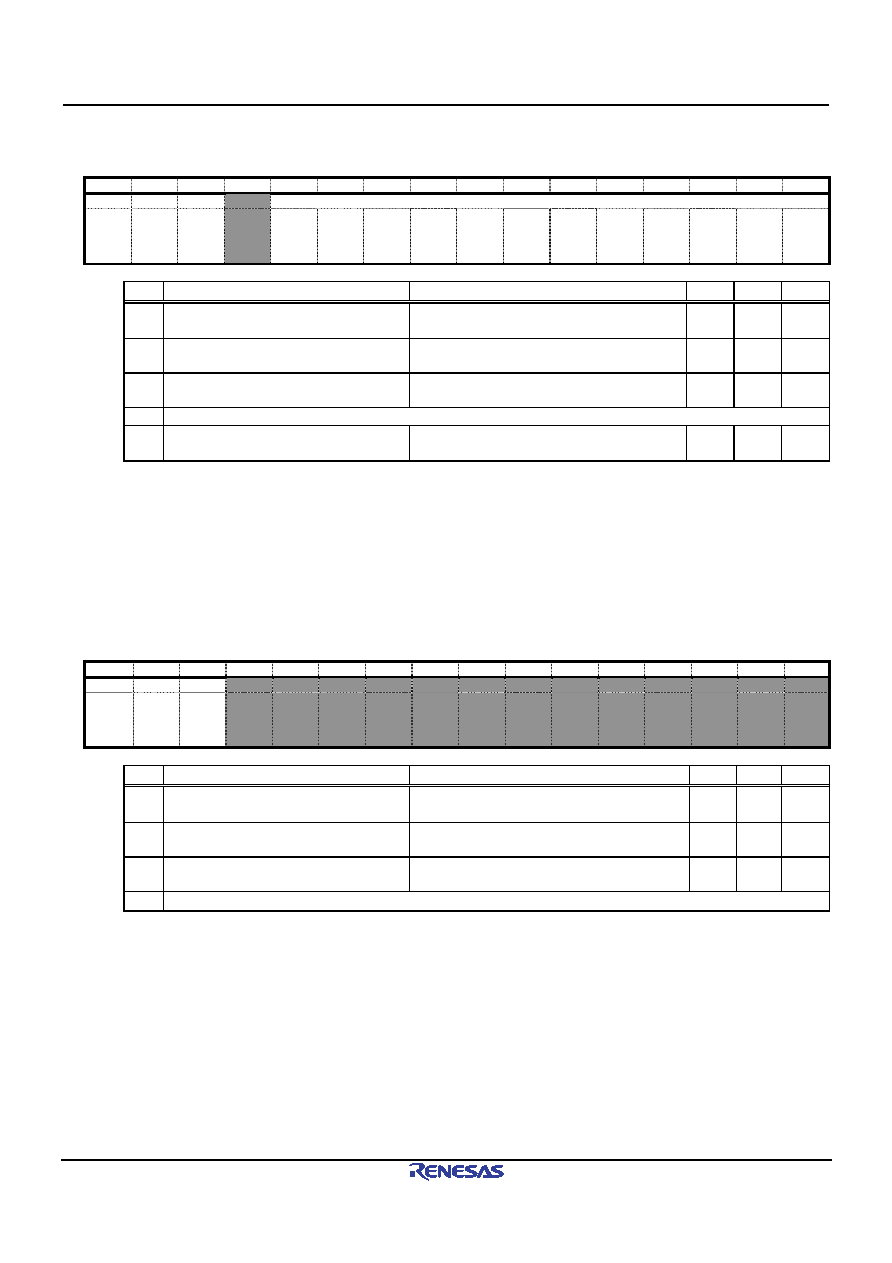
CFIFO port control register [CFIFOCTR]
<Address: 20H>
D0FIFO port control register [D0FIFOCTR]
<Address: 26H>
D1FIFO port control register [D1FIFOCTR]
<Address: 2CH>
15
14
13
12
11
10
9
8
7
6
5
4
3
2
1
0
BVAL
BCLR
FRDY
DTLN
0
-
0
-
0
-
0
?
0
-
0
-
0
-
0
-
0
-
0
-
0
-
0
-
0
-
0
-
0
-
0
-
0
Bit
Name
Function
S/W
H/W
Note
15 BVAL
Buffer Memory Valid flag
0: Invalid
1: Writing ended
R/ W(1) R/W
14 BCLR
CPU Buffer Clear
0: Invalid
1: Clears the buffer memory on the CPU side.
R(0)/
W(1)
R/W(0) 3.4.2
13 FRDY
FIFO Port Ready
0: FIFO port access is disabled.
1: The FIFO port can be accessed.
R
W
12 Nothing is placed here. This should be fixed at “0”.
11-0 DTLN
Reception Data Length
The length of the reception data can be
confirmed.
R
W
<<Notes>>
*7) Writing “1” to the BVAL bit is valid when the direction of the data packet is the sending direction (when data is
being written to the buffer memory). When the direction is the receiving direction, “BVAL=0” should be set.
*8) The BCLR bit and DTLN bit are valid for the buffer memory on the CPU side. Software should set “BCLR=1” or
refer DTLN bit after making sure that “FRDY=1”.
*9) Using the BCLR bit to clear the buffer should be done with the pipe invalid state by the pipe configuration
(“PID=NAK”).
*10) The FRDY bit requires an access cycle of at least 450 ns after the pipe has been selected.
CFIFO port SIE register [CFIFOSIE]
<Address: 22H>
15
14
13
12
11
10
9
8
7
6
5
4
3
2
1
0
TGL
SCLR SBUSY
0
-
0
-
0
-
0
?
Bit
Name
Function
S/W
H/W
Note
15 TGL
Access Right Switch
0: Invalid
1: Switches access right
R(0)/
W(1)
R/W(0) 3.4.2.3
14 SCLR
SIE Buffer Clear
0: Invalid
1: Clears buffer memory on SIE side
R(0)/
W(1)
R/W(0) 3.4.2.4
13 SBUSY
SIE Buffer Busy
0: SIE is not being accessed.
1: SIE is being accessed.
R
W
12-0 Nothing is placed here. These should be fixed at “0”.
<<Note>>
*11) The function of the TGL bit is to set the buffer memory on the SIE side to the CPU side. Set “PID=NAK” and
check the SBUSY bit to make sure the SIE is not accessing the buffer (“SBUSY=0”). Then write the TGL bit
(toggle operation). This bit is valid only for pipes for which the reception direction (reading from the buffer
memory) has been set.
*12) The function of the SCLR bit is to clear the buffer memory on the SIE side. Set “PID=NAK” and check the
SBUSY
bit to make sure the SIE is not accessing the buffer (“SBUSY=0”). Then clear the buffer. This bit is
valid only for pipes for which the sending direction (writing to the buffer memory) has been set.
相关PDF资料 |
PDF描述 |
|---|---|
| M6XXLFXI | OTHER CLOCK GENERATOR, QCC16 |
| M300LFXIT | 50 MHz, OTHER CLOCK GENERATOR, QCC16 |
| M74HC00C1R | HC/UH SERIES, QUAD 2-INPUT NAND GATE, PQCC20 |
| M74HC157B1N | HC/UH SERIES, QUAD 2 LINE TO 1 LINE MULTIPLEXER, TRUE OUTPUT, PDIP16 |
| M74HC158C1 | HC/UH SERIES, QUAD 2 LINE TO 1 LINE MULTIPLEXER, INVERTED OUTPUT, PQCC20 |
相关代理商/技术参数 |
参数描述 |
|---|---|
| M66596WG#RB0Z | 制造商:Renesas Electronics 功能描述:Tray 制造商:Renesas 功能描述:0 |
| M6668 | 制造商:Tamura Corporation of America 功能描述: |
| M66700P | 制造商:MITSUBISHI 制造商全称:Mitsubishi Electric Semiconductor 功能描述:DUAL HIGH-SPEED CCD CLOCK DRIVER |
| M66700WP | 制造商:MITSUBISHI 制造商全称:Mitsubishi Electric Semiconductor 功能描述:DUAL HIGH-SPEED CCD CLOCK DRIVER |
| M66701P | 制造商:MITSUBISHI 制造商全称:Mitsubishi Electric Semiconductor 功能描述:DUAL HIGH-SPEED CCD CLOCK DRIVER |
发布紧急采购,3分钟左右您将得到回复。