- 您现在的位置:买卖IC网 > PDF目录45052 > M66596WG UNIVERSAL SERIAL BUS CONTROLLER, PBGA64 PDF资料下载
参数资料
| 型号: | M66596WG |
| 元件分类: | 总线控制器 |
| 英文描述: | UNIVERSAL SERIAL BUS CONTROLLER, PBGA64 |
| 封装: | 0.80 MM PITCH, FBGA-64 |
| 文件页数: | 41/133页 |
| 文件大小: | 1611K |
| 代理商: | M66596WG |
第1页第2页第3页第4页第5页第6页第7页第8页第9页第10页第11页第12页第13页第14页第15页第16页第17页第18页第19页第20页第21页第22页第23页第24页第25页第26页第27页第28页第29页第30页第31页第32页第33页第34页第35页第36页第37页第38页第39页第40页当前第41页第42页第43页第44页第45页第46页第47页第48页第49页第50页第51页第52页第53页第54页第55页第56页第57页第58页第59页第60页第61页第62页第63页第64页第65页第66页第67页第68页第69页第70页第71页第72页第73页第74页第75页第76页第77页第78页第79页第80页第81页第82页第83页第84页第85页第86页第87页第88页第89页第90页第91页第92页第93页第94页第95页第96页第97页第98页第99页第100页第101页第102页第103页第104页第105页第106页第107页第108页第109页第110页第111页第112页第113页第114页第115页第116页第117页第118页第119页第120页第121页第122页第123页第124页第125页第126页第127页第128页第129页第130页第131页第132页第133页
M66596FP/WG
rev .1.00
2006.3.14
page 13 of 127
2 Registers
Reading the table of registers
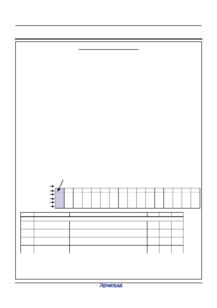
Bit no.
Each register is connected to a 16-bit internal bus.
Odd-numbered addresses will use b15 to b8, and even-numbered addresses b7 to b0.
Status after reset
This indicates the default state of the register immediately after a reset operation, and after
recovering from the low-power sleep state.
H/W Reset is the default state when an external reset signal has been input from the RST_N
pin.
S/W Reset is the default state when the user system has carried out a bit operation using the
USBE bit.
USB Reset is the default state when the controller has detected a USB bus reset.
Low-power Sleep is the default state when the controller has recovered from the low-power
sleep state.
Items that require particular attention during a reset operation are noted under “ Notes”.
“-“ indicates a state in which there is no operation by the controller, and the user setting is
retained.
“?” indicates that a value is undecided.
S/W Access Condition
This is the condition in effect if the softwear is accessing a register.
H/W Access Condition This is the condition in effect if the controller is accessing a register during any operation
other than a reset.
R ...... Read Only
W ...... Write Only
R/W ...... Read / Write
R(0) ...... "0"Read Only
W(1) ...... "1"Write Only
Note
This is the number of detailed explanations and the number of notes.
Bit Name
This indicates the bit symbol and bit name.
Function Description
This describes active items and notes.
<Example of table notation>
Nothing is placed in shaded sections. These should be fixed at “0”.
Bit number
15
14
13
12
11
10
9
8
7
6
5
4
3
2
1
0
Bit symbol
A bit B bit C bit
H/W reset
?
0
S/W reset
?
0
-
USB reset
?
0
-
Low-power sleep state
?
0
Bit
Name
Function
S/W
H/W
Note
15
Nothing is placed here. It should be fixed at “0”.
14
A bit
AAA enabled
0 : Operation disabled
1 : Operation enabled
R/W
R
2.3.1
*1
13
B bit
BBB operation
0 : "L"output
1 : "H"output
R
W
2.3.2
*1
12
C bit
CCC control
0 : .......
1 : .......
R(0)/
W(1)
R
2.3.2
<<Note>>
*1) If the A bit and B bit are being accessed in succession for writing, an access cycle of 300 ns is necessary.
相关PDF资料 |
PDF描述 |
|---|---|
| M6XXLFXI | OTHER CLOCK GENERATOR, QCC16 |
| M300LFXIT | 50 MHz, OTHER CLOCK GENERATOR, QCC16 |
| M74HC00C1R | HC/UH SERIES, QUAD 2-INPUT NAND GATE, PQCC20 |
| M74HC157B1N | HC/UH SERIES, QUAD 2 LINE TO 1 LINE MULTIPLEXER, TRUE OUTPUT, PDIP16 |
| M74HC158C1 | HC/UH SERIES, QUAD 2 LINE TO 1 LINE MULTIPLEXER, INVERTED OUTPUT, PQCC20 |
相关代理商/技术参数 |
参数描述 |
|---|---|
| M66596WG#RB0Z | 制造商:Renesas Electronics 功能描述:Tray 制造商:Renesas 功能描述:0 |
| M6668 | 制造商:Tamura Corporation of America 功能描述: |
| M66700P | 制造商:MITSUBISHI 制造商全称:Mitsubishi Electric Semiconductor 功能描述:DUAL HIGH-SPEED CCD CLOCK DRIVER |
| M66700WP | 制造商:MITSUBISHI 制造商全称:Mitsubishi Electric Semiconductor 功能描述:DUAL HIGH-SPEED CCD CLOCK DRIVER |
| M66701P | 制造商:MITSUBISHI 制造商全称:Mitsubishi Electric Semiconductor 功能描述:DUAL HIGH-SPEED CCD CLOCK DRIVER |
发布紧急采购,3分钟左右您将得到回复。