- 您现在的位置:买卖IC网 > PDF目录45052 > M66596WG UNIVERSAL SERIAL BUS CONTROLLER, PBGA64 PDF资料下载
参数资料
| 型号: | M66596WG |
| 元件分类: | 总线控制器 |
| 英文描述: | UNIVERSAL SERIAL BUS CONTROLLER, PBGA64 |
| 封装: | 0.80 MM PITCH, FBGA-64 |
| 文件页数: | 82/133页 |
| 文件大小: | 1611K |
| 代理商: | M66596WG |
第1页第2页第3页第4页第5页第6页第7页第8页第9页第10页第11页第12页第13页第14页第15页第16页第17页第18页第19页第20页第21页第22页第23页第24页第25页第26页第27页第28页第29页第30页第31页第32页第33页第34页第35页第36页第37页第38页第39页第40页第41页第42页第43页第44页第45页第46页第47页第48页第49页第50页第51页第52页第53页第54页第55页第56页第57页第58页第59页第60页第61页第62页第63页第64页第65页第66页第67页第68页第69页第70页第71页第72页第73页第74页第75页第76页第77页第78页第79页第80页第81页当前第82页第83页第84页第85页第86页第87页第88页第89页第90页第91页第92页第93页第94页第95页第96页第97页第98页第99页第100页第101页第102页第103页第104页第105页第106页第107页第108页第109页第110页第111页第112页第113页第114页第115页第116页第117页第118页第119页第120页第121页第122页第123页第124页第125页第126页第127页第128页第129页第130页第131页第132页第133页
M66596FP/WG
rev .1.00
2006.3.14
page 50 of 127
3.1.5
USB data bus resistor control
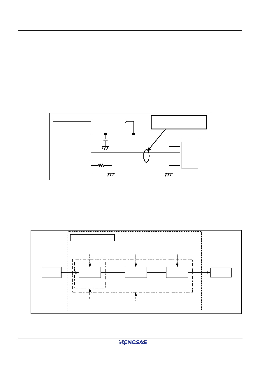
Figure 3.1 shows a diagram of the connections between the controller and the USB connectors.
For the Peripheral mode, the controller has a built-in pull-up resistor for the D+ signal. “1” should be set for the
DPRPU
bit of the SYSCFG register, then the D+ line is pulled up. The pull-up power supply is AFE33V.
For the Host mode, the controller has a built-in pull-down resistor for the D+ and D- signals. “1” should be set for
the DPRPD bit of the SYSCFG register, then the D+ and D- lines are pulled down.
Also, the controller has a built-in terminal resistor for use when the D+ and D- signals are operating at Hi-Speed,
and a built-in output resistor for Full-Speed operation. The controller automatically switches the built-in resistor
after connection with the PC, by means of reset handshake, suspended state and resume detection. If a disconnection
from the PC is detected, the H/W should be initialized by means of an S/W reset (USBE=0).
If “0” is set for the DPRPU bit of the SYSCFG register in the Peripheral mode, the pull-up resistor (or the terminal
resistor) of the USB data line is disabled, making it possible to notify the host controller of the device disconnection.
M66596
VBUS
USB connector
1
3
2
4 GND
D-
D+
Vbus
DM
DP
RERFIN
5.6K
Impedance control has to be taken into
consideration when designing the D+
and D- lines.
+5V
(at the Host mode)
Figure 3.1 UBS connector connections
3.1.6
Clock supply control
Figure 3.2 shows a block diagram of the controller clock control. Frequency of the input clock for the XIN pin
should be selected using the XTAL bit of the SYSCFG register, while the oscillation buffer is enabled using the XCKE
bit and the clock supply is controlled using the RCKE, PLLC, and SCKE bits. For information on the register control
timing, please refer to 3.1.8, State transition timing.
Auto clock supply
Low-power
control
Input
clock
Oscillation
buffer
XCKE
(bit13)
PLLC, SCKE
(bit11, bit10)
Internal
clock
PLL
Clock control unit
RCKE
(bit12)
Divider
circuit
PCUT
(bit1)
ATCKM
(bit8)
Figure 3.2 Clock control block
相关PDF资料 |
PDF描述 |
|---|---|
| M6XXLFXI | OTHER CLOCK GENERATOR, QCC16 |
| M300LFXIT | 50 MHz, OTHER CLOCK GENERATOR, QCC16 |
| M74HC00C1R | HC/UH SERIES, QUAD 2-INPUT NAND GATE, PQCC20 |
| M74HC157B1N | HC/UH SERIES, QUAD 2 LINE TO 1 LINE MULTIPLEXER, TRUE OUTPUT, PDIP16 |
| M74HC158C1 | HC/UH SERIES, QUAD 2 LINE TO 1 LINE MULTIPLEXER, INVERTED OUTPUT, PQCC20 |
相关代理商/技术参数 |
参数描述 |
|---|---|
| M66596WG#RB0Z | 制造商:Renesas Electronics 功能描述:Tray 制造商:Renesas 功能描述:0 |
| M6668 | 制造商:Tamura Corporation of America 功能描述: |
| M66700P | 制造商:MITSUBISHI 制造商全称:Mitsubishi Electric Semiconductor 功能描述:DUAL HIGH-SPEED CCD CLOCK DRIVER |
| M66700WP | 制造商:MITSUBISHI 制造商全称:Mitsubishi Electric Semiconductor 功能描述:DUAL HIGH-SPEED CCD CLOCK DRIVER |
| M66701P | 制造商:MITSUBISHI 制造商全称:Mitsubishi Electric Semiconductor 功能描述:DUAL HIGH-SPEED CCD CLOCK DRIVER |
发布紧急采购,3分钟左右您将得到回复。