- 您现在的位置:买卖IC网 > PDF目录45052 > M66596WG UNIVERSAL SERIAL BUS CONTROLLER, PBGA64 PDF资料下载
参数资料
| 型号: | M66596WG |
| 元件分类: | 总线控制器 |
| 英文描述: | UNIVERSAL SERIAL BUS CONTROLLER, PBGA64 |
| 封装: | 0.80 MM PITCH, FBGA-64 |
| 文件页数: | 81/133页 |
| 文件大小: | 1611K |
| 代理商: | M66596WG |
第1页第2页第3页第4页第5页第6页第7页第8页第9页第10页第11页第12页第13页第14页第15页第16页第17页第18页第19页第20页第21页第22页第23页第24页第25页第26页第27页第28页第29页第30页第31页第32页第33页第34页第35页第36页第37页第38页第39页第40页第41页第42页第43页第44页第45页第46页第47页第48页第49页第50页第51页第52页第53页第54页第55页第56页第57页第58页第59页第60页第61页第62页第63页第64页第65页第66页第67页第68页第69页第70页第71页第72页第73页第74页第75页第76页第77页第78页第79页第80页当前第81页第82页第83页第84页第85页第86页第87页第88页第89页第90页第91页第92页第93页第94页第95页第96页第97页第98页第99页第100页第101页第102页第103页第104页第105页第106页第107页第108页第109页第110页第111页第112页第113页第114页第115页第116页第117页第118页第119页第120页第121页第122页第123页第124页第125页第126页第127页第128页第129页第130页第131页第132页第133页
M66596FP/WG
rev .1.00
2006.3.14
page 49 of 127
3 Description of Operation
3.1 System control and oscillation control
This chapter describes the register operations that are necessary to the default settings of the controller, and the
registers necessary for power consumption control.
3.1.1
Resets
Table 3.1 shows a table of controller resets. For information on the initialized states of the registers following the
various reset operations, please refer to Chapter 2, Registers.
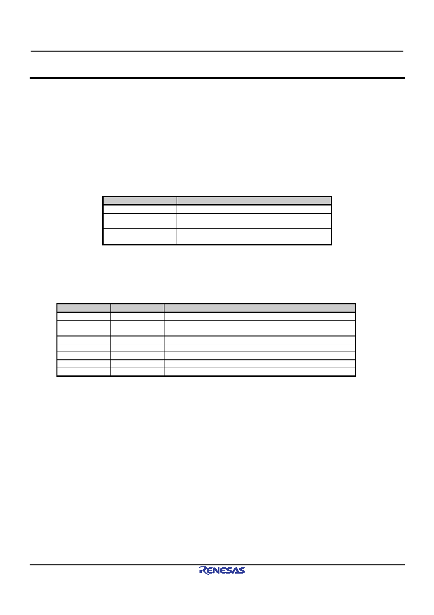
Table 3.1 Types of Resets
Name
Operation
H/W reset
”L” level input from the RST_N pin
S/W reset
Operation using the USBE bit of the SYSCFG
register
USB bus reset
Automatically detected by the controller from the
D+ and D- lines in tne Peripheral mode
3.1.2
Bus interface settings
Table 3.2 shows the bus interface settings for the controller.
Table 3.2 Bus interface settings
Register name
Bit name
Setting contents
PINCFG
LDRV
Control setting for the drive current
PINCFG
BIGEND
Byte Endian setting for the CPU being connected
This bit is effective in access to a FIFO register
DMAxCFG
DREQA
Active setting for the DREQx_N pin
DMAxCFG
DACKA
Active setting for the DACKx_N pin
DMAxCFG
DENDA
Active setting for the DENDx_N pin
DMAxCFG
OBUS
OBUS mode setting
INTENB1
INTL
Output sensing setting for the INT_N pin
3.1.3
Selection of the function
This controller can select either a Host function or a Peripheral function by software. To select USB function for
the controller, set the DCFM bit of the SYSCFG register. Changing the DCFM bit (writing access) should be done
with the internal clock stopped (“SCKE=0”).
3.1.4
Enabling Hi-Speed operation
With this controller, either Hi-Speed operation or Full-Speed operation can be selected as the USB communication
speed (communication bit rate), using software. To enable Hi-Speed operation for the controller, set the HSE bit of
the SYSCFG register to “1”. Changing the HSE bit should be done with the internal clock stopped (“SCKE=0”).
If Hi-Speed operation has been enabled, the controller executes the reset handshake protocol, and the USB
communication speed is set automatically. The results of the reset handshake can be confirmed using the RHST bit
of the DVSTCTR register.
If Hi-Speed operation has been disabled, the controller will use Full-Speed operation.
相关PDF资料 |
PDF描述 |
|---|---|
| M6XXLFXI | OTHER CLOCK GENERATOR, QCC16 |
| M300LFXIT | 50 MHz, OTHER CLOCK GENERATOR, QCC16 |
| M74HC00C1R | HC/UH SERIES, QUAD 2-INPUT NAND GATE, PQCC20 |
| M74HC157B1N | HC/UH SERIES, QUAD 2 LINE TO 1 LINE MULTIPLEXER, TRUE OUTPUT, PDIP16 |
| M74HC158C1 | HC/UH SERIES, QUAD 2 LINE TO 1 LINE MULTIPLEXER, INVERTED OUTPUT, PQCC20 |
相关代理商/技术参数 |
参数描述 |
|---|---|
| M66596WG#RB0Z | 制造商:Renesas Electronics 功能描述:Tray 制造商:Renesas 功能描述:0 |
| M6668 | 制造商:Tamura Corporation of America 功能描述: |
| M66700P | 制造商:MITSUBISHI 制造商全称:Mitsubishi Electric Semiconductor 功能描述:DUAL HIGH-SPEED CCD CLOCK DRIVER |
| M66700WP | 制造商:MITSUBISHI 制造商全称:Mitsubishi Electric Semiconductor 功能描述:DUAL HIGH-SPEED CCD CLOCK DRIVER |
| M66701P | 制造商:MITSUBISHI 制造商全称:Mitsubishi Electric Semiconductor 功能描述:DUAL HIGH-SPEED CCD CLOCK DRIVER |
发布紧急采购,3分钟左右您将得到回复。