- 您现在的位置:买卖IC网 > PDF目录45052 > M66596WG UNIVERSAL SERIAL BUS CONTROLLER, PBGA64 PDF资料下载
参数资料
| 型号: | M66596WG |
| 元件分类: | 总线控制器 |
| 英文描述: | UNIVERSAL SERIAL BUS CONTROLLER, PBGA64 |
| 封装: | 0.80 MM PITCH, FBGA-64 |
| 文件页数: | 101/133页 |
| 文件大小: | 1611K |
| 代理商: | M66596WG |
第1页第2页第3页第4页第5页第6页第7页第8页第9页第10页第11页第12页第13页第14页第15页第16页第17页第18页第19页第20页第21页第22页第23页第24页第25页第26页第27页第28页第29页第30页第31页第32页第33页第34页第35页第36页第37页第38页第39页第40页第41页第42页第43页第44页第45页第46页第47页第48页第49页第50页第51页第52页第53页第54页第55页第56页第57页第58页第59页第60页第61页第62页第63页第64页第65页第66页第67页第68页第69页第70页第71页第72页第73页第74页第75页第76页第77页第78页第79页第80页第81页第82页第83页第84页第85页第86页第87页第88页第89页第90页第91页第92页第93页第94页第95页第96页第97页第98页第99页第100页当前第101页第102页第103页第104页第105页第106页第107页第108页第109页第110页第111页第112页第113页第114页第115页第116页第117页第118页第119页第120页第121页第122页第123页第124页第125页第126页第127页第128页第129页第130页第131页第132页第133页
M66596FP/WG
rev .1.00
2006.3.14
page 5 of 127
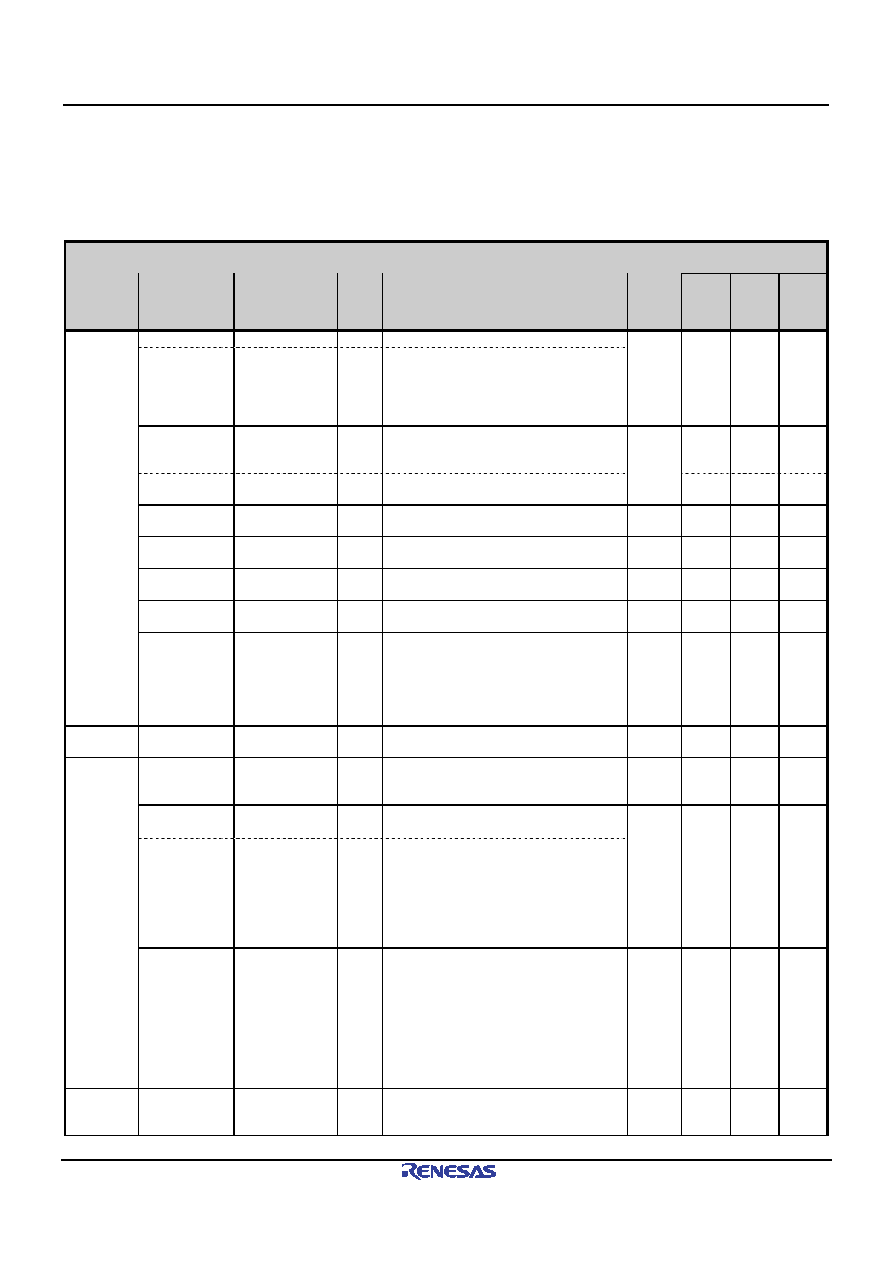
1.4 Description of pins
Table 1.1 describes the controller pins. Table 1.2 describes the not used pins.
Table 1.1 Pin descriptions
State of pin *7)
Category
Pin name
Name
I/O
Function
Pin
count
(Pin
no.s.)
RST_
N=”L”
RST_
N
goes
“H”
PCUT
=1
D15-0
Data Bus
I/O
This is a 16-bit data bus.
AD6-1
Multiplex
Address Bus
I/O
When a multiplex bus is specified, this
group of pins is used on a time-shared
basis for some of the data buses
(D6-D1), or for 6 bits of the address
bus (A6-A1).
16
(24-39)
Input
(Hi-z)
A6-1
Address Bus
IN
This is a 6-bit address bus.
Because the data bus consists of 16
bits, there is no A0.
Input
Input
Input
(Hi-z)
ALE
Address Latch
Enable
IN
When a multiplex bus is specified, the
A6 pin is used as the ALE signal.
6
(18-23)
Input
CS_N
Chip Select
IN
Setting this to the “L” level selects this
controller.
1
(56)
Input
Input
Input
RD_N
Read Strobe
IN
Setting this to the “L” level reads data
from the controller registers.
1
(53)
Input
WR0_N
D7-0 Byte
Write Strobe
IN
At the rising edge, D7-D0 are written to
the registers of the controller.
1
(54)
Input
Input
Input
WR1_N
D15-8 Byte
Write Strobe
IN
At the rising edge, D15-D8 are written
to the registers of the controller.
1
(55)
Input
Input
Input
CPU bus
interface
MPBUS
Bus Mode
Selection
IN
Setting this to the “L” level selects a
separate bus.
Setting this to the “H” level selects a
multiplex bus.
This should be fixed at either the “H” or
“L” level.
1
(17)
Input
Input
Input
Split bus
interface
SD7-0
Split Data Bus
I/O
If a split bus is selected, this functions
as the data bus for the split bus.
8
(43-50)
Input
(Hi-z)
Input
(Hi-z)
Input
(Hi-z)
DREQ0_N*1)
DREQ1_N*1)
DMA Request
OUT
This notifies the system of a D0FIFO
port or D1FIFO port DMA transfer
request.
2
(57, 60)
H
H/L
DACK0_N*1)
DACK1_N*1)
DMA
Acknowledge
IN
Input the DMA Acknowledge signal for
the D0FIFO or D1FIFO port.
DSTB0_N*2)
Data Strobe 0
IN
This functions as the data strobe
signal for the D0FIFO port.
Because it is also used for the DMA
Acknowledge signal of the D1FIFO
port, the DSTB0_N function cannot be
used if the DACK1_N function is being
used.
2
(58, 61)
Input
DMA bus
interface
DEND0_N*1)
DEND1_N*1)
DMA Transfer
End
I/O
<In the FIFO port access writing
direction>
This receives the Transfer End signal
from another peripheral chip or the
CPU as an input signal.
<In the FIFO port access reading
direction>
This indicates the transfer end data as
an output signal.
2
(59, 62)
Input
(Hi-z)
Input
(Hi-z)
Input
(Hi-z)
Interrupt/
SOF
output
INT_N
Interrupt
OUT
In the “L” active state, this notifies the
system of various types of interrupts
relating to USB communication.
1
(51)
H
相关PDF资料 |
PDF描述 |
|---|---|
| M6XXLFXI | OTHER CLOCK GENERATOR, QCC16 |
| M300LFXIT | 50 MHz, OTHER CLOCK GENERATOR, QCC16 |
| M74HC00C1R | HC/UH SERIES, QUAD 2-INPUT NAND GATE, PQCC20 |
| M74HC157B1N | HC/UH SERIES, QUAD 2 LINE TO 1 LINE MULTIPLEXER, TRUE OUTPUT, PDIP16 |
| M74HC158C1 | HC/UH SERIES, QUAD 2 LINE TO 1 LINE MULTIPLEXER, INVERTED OUTPUT, PQCC20 |
相关代理商/技术参数 |
参数描述 |
|---|---|
| M66596WG#RB0Z | 制造商:Renesas Electronics 功能描述:Tray 制造商:Renesas 功能描述:0 |
| M6668 | 制造商:Tamura Corporation of America 功能描述: |
| M66700P | 制造商:MITSUBISHI 制造商全称:Mitsubishi Electric Semiconductor 功能描述:DUAL HIGH-SPEED CCD CLOCK DRIVER |
| M66700WP | 制造商:MITSUBISHI 制造商全称:Mitsubishi Electric Semiconductor 功能描述:DUAL HIGH-SPEED CCD CLOCK DRIVER |
| M66701P | 制造商:MITSUBISHI 制造商全称:Mitsubishi Electric Semiconductor 功能描述:DUAL HIGH-SPEED CCD CLOCK DRIVER |
发布紧急采购,3分钟左右您将得到回复。