- 您现在的位置:买卖IC网 > PDF目录45052 > M66596WG UNIVERSAL SERIAL BUS CONTROLLER, PBGA64 PDF资料下载
参数资料
| 型号: | M66596WG |
| 元件分类: | 总线控制器 |
| 英文描述: | UNIVERSAL SERIAL BUS CONTROLLER, PBGA64 |
| 封装: | 0.80 MM PITCH, FBGA-64 |
| 文件页数: | 47/133页 |
| 文件大小: | 1611K |
| 代理商: | M66596WG |
第1页第2页第3页第4页第5页第6页第7页第8页第9页第10页第11页第12页第13页第14页第15页第16页第17页第18页第19页第20页第21页第22页第23页第24页第25页第26页第27页第28页第29页第30页第31页第32页第33页第34页第35页第36页第37页第38页第39页第40页第41页第42页第43页第44页第45页第46页当前第47页第48页第49页第50页第51页第52页第53页第54页第55页第56页第57页第58页第59页第60页第61页第62页第63页第64页第65页第66页第67页第68页第69页第70页第71页第72页第73页第74页第75页第76页第77页第78页第79页第80页第81页第82页第83页第84页第85页第86页第87页第88页第89页第90页第91页第92页第93页第94页第95页第96页第97页第98页第99页第100页第101页第102页第103页第104页第105页第106页第107页第108页第109页第110页第111页第112页第113页第114页第115页第116页第117页第118页第119页第120页第121页第122页第123页第124页第125页第126页第127页第128页第129页第130页第131页第132页第133页
M66596FP/WG
rev .1.00
2006.3.14
page 18 of 127
2.3 System control
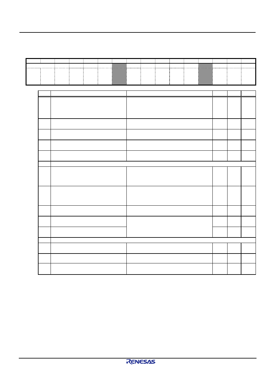
System configuration control register [SYSCFG]
<Address : 00H>
15
14
13
12
11
10
9
8
7
6
5
4
3
2
1
0
XTAL
XCKE
RCKE
PLLC
SCKE
ATCKM
HSE
DCFM DMRPD DPRPU
FSRPC PCUT
USBE
0
-
0
-
0
-
1
0
-
0
-
0
-
0
?
0
-
0
-
0
-
0
-
0
-
?
0
-
0
-
0
-
Bit
Name
Function
S/W
H/W
Note
15-14 XTAL
Clock selection
00: 12 MHz input
01: 24 MHz input
10: 48 MHz input
11: Reserved
R/W
R
13
XCKE
Oscillation buffer enabled
0: Oscillation buffer operation disabled
1: Oscillation buffer operation enabled
R/W
(1)
12
RCKE
Reference clock enabled
0: Reference clock supply stopped
1: Reference clock supply enabled
R/W
R
11
PLLC
PLL operation enabled
0: PLL operation disabled
1: PLL operation enabled
R/W
R
10
SCKE
Internal clock enabled
0: Internal clock supply stopped
1: Internal clock supply enabled
R/W
R
9
Nothing is placed here. It should be fixed at “0”.
8
ATCKM
Auto clock supply function enabled
The clock is supplied from the low-power sleep
state or clock stop state.
0: Auto clock supply function disabled
1: Auto clock supply function enabled
R/W
R
7
HSE
Hi-Speed operation enabled
This enables Hi-Speed operation.
0: Hi-Speed operation disabled (Full-Speed)
1: Hi-Speed operation enabled (detected by
controller)
R/W
R
6
DCFM
0: Peripheral Controller
1: Host Controller
R/W
R
5
DMRPD
D+,D- line resistance control
R/W
R
4
DPRPU
D+,D- line resistance control
For detailed information, refer to Chapter 2.3.4
R/W
R
3
Nothing is placed here. These should be fixed at “0”.
2
FSRPC
Full-Speed receiver enable
0: Full-Speed receiver is controled by H/W
1: Full-Speed receiver enabled by S/W
R/W
R
1
PCUT
Low-power sleep state enabled
0: Normal operation state
1: Low-power sleep state
R/W (1) R/W
(0)
0
USBE
USB block operation enabled
0: USB block operation disabled (S/W Reset)
1: USB block operation enabled
R/W
R
<< Notes >>
*1) The Hi-Speed operation enabled (HSE) bit and Device Controller function (DCFM) should be set before the
internal clock is supplied and .setup DPRPU and DPRPD bit.
*2) When the system returns from the low-power sleep state to the normal operation state, the controller sets
“XCKE = 1”.
相关PDF资料 |
PDF描述 |
|---|---|
| M6XXLFXI | OTHER CLOCK GENERATOR, QCC16 |
| M300LFXIT | 50 MHz, OTHER CLOCK GENERATOR, QCC16 |
| M74HC00C1R | HC/UH SERIES, QUAD 2-INPUT NAND GATE, PQCC20 |
| M74HC157B1N | HC/UH SERIES, QUAD 2 LINE TO 1 LINE MULTIPLEXER, TRUE OUTPUT, PDIP16 |
| M74HC158C1 | HC/UH SERIES, QUAD 2 LINE TO 1 LINE MULTIPLEXER, INVERTED OUTPUT, PQCC20 |
相关代理商/技术参数 |
参数描述 |
|---|---|
| M66596WG#RB0Z | 制造商:Renesas Electronics 功能描述:Tray 制造商:Renesas 功能描述:0 |
| M6668 | 制造商:Tamura Corporation of America 功能描述: |
| M66700P | 制造商:MITSUBISHI 制造商全称:Mitsubishi Electric Semiconductor 功能描述:DUAL HIGH-SPEED CCD CLOCK DRIVER |
| M66700WP | 制造商:MITSUBISHI 制造商全称:Mitsubishi Electric Semiconductor 功能描述:DUAL HIGH-SPEED CCD CLOCK DRIVER |
| M66701P | 制造商:MITSUBISHI 制造商全称:Mitsubishi Electric Semiconductor 功能描述:DUAL HIGH-SPEED CCD CLOCK DRIVER |
发布紧急采购,3分钟左右您将得到回复。