- 您现在的位置:买卖IC网 > PDF目录45052 > M66596WG UNIVERSAL SERIAL BUS CONTROLLER, PBGA64 PDF资料下载
参数资料
| 型号: | M66596WG |
| 元件分类: | 总线控制器 |
| 英文描述: | UNIVERSAL SERIAL BUS CONTROLLER, PBGA64 |
| 封装: | 0.80 MM PITCH, FBGA-64 |
| 文件页数: | 9/133页 |
| 文件大小: | 1611K |
| 代理商: | M66596WG |
第1页第2页第3页第4页第5页第6页第7页第8页当前第9页第10页第11页第12页第13页第14页第15页第16页第17页第18页第19页第20页第21页第22页第23页第24页第25页第26页第27页第28页第29页第30页第31页第32页第33页第34页第35页第36页第37页第38页第39页第40页第41页第42页第43页第44页第45页第46页第47页第48页第49页第50页第51页第52页第53页第54页第55页第56页第57页第58页第59页第60页第61页第62页第63页第64页第65页第66页第67页第68页第69页第70页第71页第72页第73页第74页第75页第76页第77页第78页第79页第80页第81页第82页第83页第84页第85页第86页第87页第88页第89页第90页第91页第92页第93页第94页第95页第96页第97页第98页第99页第100页第101页第102页第103页第104页第105页第106页第107页第108页第109页第110页第111页第112页第113页第114页第115页第116页第117页第118页第119页第120页第121页第122页第123页第124页第125页第126页第127页第128页第129页第130页第131页第132页第133页
M66596FP/WG
rev .1.00
2006.3.14
page 104 of 127
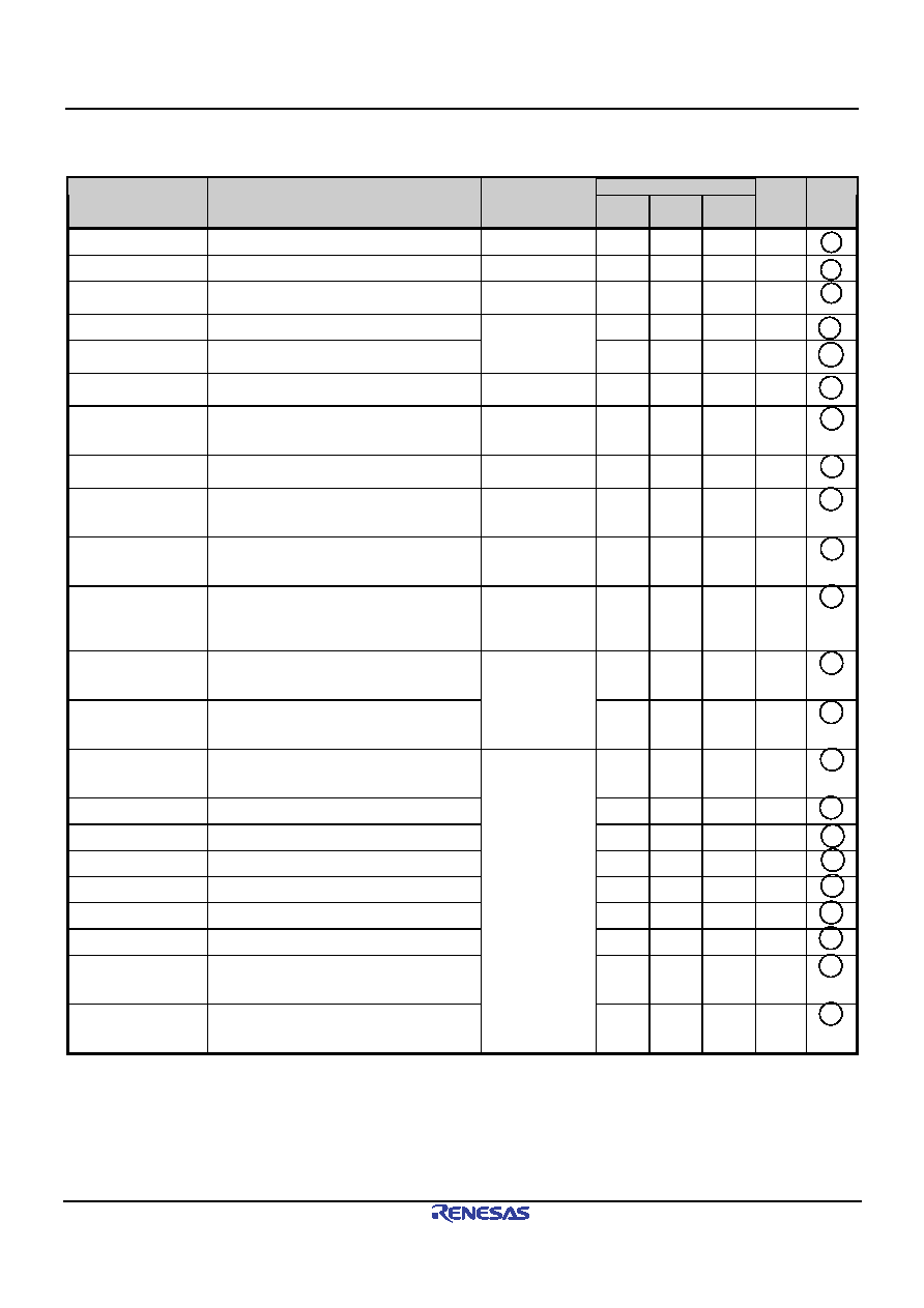
4.7 Switching characteristics (VIF = 2.7~3.6V, or 1.6~2.0V)
Rated value
Symbol
Item
Measurement
conditions /
other
Min.
Typ.
Max.
Unit
Ref.
no.
ta (A)
Address access time
CL=50 pF
40
ns
1
tv (A)
Time that data is valid after address
CL=10 pF
2
ns
2
ta (CTRL - D)
Time that data can be accessed after
control
CL=50 pF
30
ns
3
tv (CTRL - D)
Time that data is valid after control
CL=10 pF
2
ns
4
ten (CTRL - D)
Time that data output is enabled after
control
2
ns
5
tdis (CTRL - D)
Time that data output is disabled after
control
CL=50 pF
30
ns
6
ta (CTRL - DV)
Time that data can be accessed after
control when split bus (DMA Interface)
Obus=0
CL=30 pF
30
ns
9
tv (CTRL – DV)
Time that data can is valid after control
when split bus (DMA Interface) Obus=0
CL=10 pF
2
ns
10
ta (CTRL - DendV)
Time that DEND output can be accessed
after control when split bus (DMA
Interface) Obus=0
CL=30 pF
30
ns
11
tv (CTRL - DendV)
Time that DEND output is valid after
control when CPU bus and split bus
(DMA Interface) Obus=0
CL=10 pF
2
ns
12
ta (CTRL - Dend)
Time that DEND output can be accessed
after control when split bus (DMA
Interface) Obus=1
CL=30 pF
30
ns
13
tv (CTRL – Dend)
Time that DEND output is valid after
control when CPU bus and split bus
(DMA Interface) Obus=1
CL=10 pF
2
ns
14
ten (CTRL – Dend)
Time that DEND output is enabled after
control when CPU bus and split bus
(DMA Interface) Obus=1
2
ns
15
tdis (CTRL-Dend)
Time that DEND output is disabled after
control when CPU bus and split bus
(DMA Interface) Obus=1
CL=30 pF
30
ns
16
tdis (CTRL – Dreq)
Time that DREQ is disabled after control
70
ns
17
tdis (CTRLH –Dreq)
Time that DREQ is disabled after control
70
ns
18
ten (CTRL – Dreq)
Time that DREQ is enabled after control
30
ns
19
twh (Dreq)
DREQ output "H" pulse width
20
50
ns
20
td (CTRL - INT)
INT output negated delay time
250
ns
21
twh (INT)
INT output “H” pulse width
650
ns
22
td (DREQ - DV)
Data access after DREQ begins to be
asserted when split bus (DMA Interface)
Obus=0
0
ns
23
td (DREQ - DendV)
Time that DEND can be accessed after
DREQ begins to be asserted when split
bus (DMA Interface) Obus=0
0
ns
24
Key
ta: Access time, tv: Valid time, ten: Output enabled time, tdis: Output disabled time, td: propagation delay
(A): Address, (D): Data, (Dend): DEND, (CTRL): Control, (V): Obus=0
相关PDF资料 |
PDF描述 |
|---|---|
| M6XXLFXI | OTHER CLOCK GENERATOR, QCC16 |
| M300LFXIT | 50 MHz, OTHER CLOCK GENERATOR, QCC16 |
| M74HC00C1R | HC/UH SERIES, QUAD 2-INPUT NAND GATE, PQCC20 |
| M74HC157B1N | HC/UH SERIES, QUAD 2 LINE TO 1 LINE MULTIPLEXER, TRUE OUTPUT, PDIP16 |
| M74HC158C1 | HC/UH SERIES, QUAD 2 LINE TO 1 LINE MULTIPLEXER, INVERTED OUTPUT, PQCC20 |
相关代理商/技术参数 |
参数描述 |
|---|---|
| M66596WG#RB0Z | 制造商:Renesas Electronics 功能描述:Tray 制造商:Renesas 功能描述:0 |
| M6668 | 制造商:Tamura Corporation of America 功能描述: |
| M66700P | 制造商:MITSUBISHI 制造商全称:Mitsubishi Electric Semiconductor 功能描述:DUAL HIGH-SPEED CCD CLOCK DRIVER |
| M66700WP | 制造商:MITSUBISHI 制造商全称:Mitsubishi Electric Semiconductor 功能描述:DUAL HIGH-SPEED CCD CLOCK DRIVER |
| M66701P | 制造商:MITSUBISHI 制造商全称:Mitsubishi Electric Semiconductor 功能描述:DUAL HIGH-SPEED CCD CLOCK DRIVER |
发布紧急采购,3分钟左右您将得到回复。