- 您现在的位置:买卖IC网 > PDF目录45052 > M66596WG UNIVERSAL SERIAL BUS CONTROLLER, PBGA64 PDF资料下载
参数资料
| 型号: | M66596WG |
| 元件分类: | 总线控制器 |
| 英文描述: | UNIVERSAL SERIAL BUS CONTROLLER, PBGA64 |
| 封装: | 0.80 MM PITCH, FBGA-64 |
| 文件页数: | 31/133页 |
| 文件大小: | 1611K |
| 代理商: | M66596WG |
第1页第2页第3页第4页第5页第6页第7页第8页第9页第10页第11页第12页第13页第14页第15页第16页第17页第18页第19页第20页第21页第22页第23页第24页第25页第26页第27页第28页第29页第30页当前第31页第32页第33页第34页第35页第36页第37页第38页第39页第40页第41页第42页第43页第44页第45页第46页第47页第48页第49页第50页第51页第52页第53页第54页第55页第56页第57页第58页第59页第60页第61页第62页第63页第64页第65页第66页第67页第68页第69页第70页第71页第72页第73页第74页第75页第76页第77页第78页第79页第80页第81页第82页第83页第84页第85页第86页第87页第88页第89页第90页第91页第92页第93页第94页第95页第96页第97页第98页第99页第100页第101页第102页第103页第104页第105页第106页第107页第108页第109页第110页第111页第112页第113页第114页第115页第116页第117页第118页第119页第120页第121页第122页第123页第124页第125页第126页第127页第128页第129页第130页第131页第132页第133页
M66596FP/WG
rev .1.00
2006.3.14
page 124 of 127
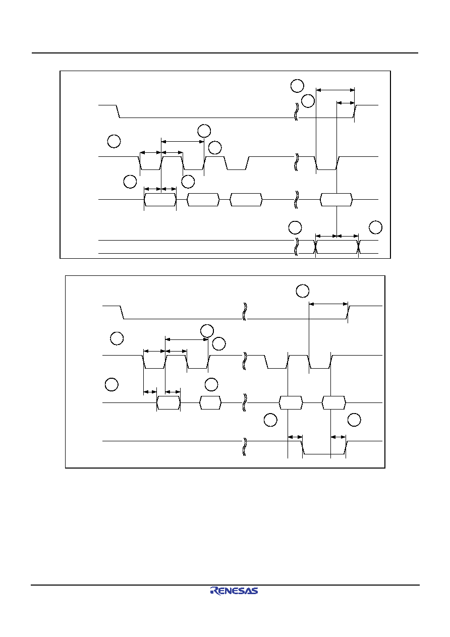
4.9.5.11 DMA Burst transfer write timing (CPU bus address not used: DFORM=011)
18
tdis (CTRLH - Dreq)
tw (CTRL_B)
48
tsu (D) th (D)
43
44
DREQi_N
(i=0,1)
D15-D0
D0
tsu (Dend) th (Dend)
45
46
DENDi_N
(i=0,1)
trec (CTRL_B)
tw (cycle)
49
47
D1
Dn
D2
DACKi_N
(i=0,1)
17 tdis (CTRL - Dreq)
4.9.5.12 DMA burst transfer read timing (CPU bus address not used: DFORM=011)
17
tdis (CTRL - Dreq)
tw (CTRL_B)
48
ta (CTRL - D)
tv (CTRL - D)
4
3
DREQi_N
(i=0,1)
DACKi_N
(i=0,1)
D15-D0
D0
ta (CTRL - DendV)
tv (CTRL - DendV)
12
DENDi _N
(i=0,1)
trec (CTRL_B)
tw (cycle)
49
47
D1
11
Dn-1
Dn
Note 5-6
Note 5-1: The control signal when writing data is a combination of DACKi_N(i=0, 1), WR0_N and WR1_N.
Note 5-2: The control signal when reading data is a combination of DACKi_N and RD_N.
Note 5-3: The control signal when writing data is a combination of DACK0 and DSTRB0_N.
Note 5-4: The control signal when writing data is a combination of CS_N, WR0_N and WR1_N.
Note 5-5: The control signal when reading data is a combination of CS_N and RD_N.
Note 5-6: When the receipt data is one byte, the data determined time is "(23)td(DREQ-DV)" and the DEND determined
time is "(24)td(DREQ-DendV)".
Note 5-7: RD_N, WR0_N and WR1_N should not be timed to fall at the same time that CS_N is rising. Similarly, CS_N
should not be timed to fall at the same timing that RD_N, WR0_N and WR1_N are rising. In the instances noted
above, an interval must be needed at least 10ns.
Note 5-8:. RD_N, WR0_N and WR1_N should not be timed to fall at the same time that DACKi_N is rising. Similarly,
DACKi_N should not be timed to fall at the same timing that RD_N, WR0_N and WR1_N are rising. In the
instances noted above, an interval must be needed at least 10ns.
相关PDF资料 |
PDF描述 |
|---|---|
| M6XXLFXI | OTHER CLOCK GENERATOR, QCC16 |
| M300LFXIT | 50 MHz, OTHER CLOCK GENERATOR, QCC16 |
| M74HC00C1R | HC/UH SERIES, QUAD 2-INPUT NAND GATE, PQCC20 |
| M74HC157B1N | HC/UH SERIES, QUAD 2 LINE TO 1 LINE MULTIPLEXER, TRUE OUTPUT, PDIP16 |
| M74HC158C1 | HC/UH SERIES, QUAD 2 LINE TO 1 LINE MULTIPLEXER, INVERTED OUTPUT, PQCC20 |
相关代理商/技术参数 |
参数描述 |
|---|---|
| M66596WG#RB0Z | 制造商:Renesas Electronics 功能描述:Tray 制造商:Renesas 功能描述:0 |
| M6668 | 制造商:Tamura Corporation of America 功能描述: |
| M66700P | 制造商:MITSUBISHI 制造商全称:Mitsubishi Electric Semiconductor 功能描述:DUAL HIGH-SPEED CCD CLOCK DRIVER |
| M66700WP | 制造商:MITSUBISHI 制造商全称:Mitsubishi Electric Semiconductor 功能描述:DUAL HIGH-SPEED CCD CLOCK DRIVER |
| M66701P | 制造商:MITSUBISHI 制造商全称:Mitsubishi Electric Semiconductor 功能描述:DUAL HIGH-SPEED CCD CLOCK DRIVER |
发布紧急采购,3分钟左右您将得到回复。