- 您现在的位置:买卖IC网 > PDF目录45052 > M66596WG UNIVERSAL SERIAL BUS CONTROLLER, PBGA64 PDF资料下载
参数资料
| 型号: | M66596WG |
| 元件分类: | 总线控制器 |
| 英文描述: | UNIVERSAL SERIAL BUS CONTROLLER, PBGA64 |
| 封装: | 0.80 MM PITCH, FBGA-64 |
| 文件页数: | 113/133页 |
| 文件大小: | 1611K |
| 代理商: | M66596WG |
第1页第2页第3页第4页第5页第6页第7页第8页第9页第10页第11页第12页第13页第14页第15页第16页第17页第18页第19页第20页第21页第22页第23页第24页第25页第26页第27页第28页第29页第30页第31页第32页第33页第34页第35页第36页第37页第38页第39页第40页第41页第42页第43页第44页第45页第46页第47页第48页第49页第50页第51页第52页第53页第54页第55页第56页第57页第58页第59页第60页第61页第62页第63页第64页第65页第66页第67页第68页第69页第70页第71页第72页第73页第74页第75页第76页第77页第78页第79页第80页第81页第82页第83页第84页第85页第86页第87页第88页第89页第90页第91页第92页第93页第94页第95页第96页第97页第98页第99页第100页第101页第102页第103页第104页第105页第106页第107页第108页第109页第110页第111页第112页当前第113页第114页第115页第116页第117页第118页第119页第120页第121页第122页第123页第124页第125页第126页第127页第128页第129页第130页第131页第132页第133页
M66596FP/WG
rev .1.00
2006.3.14
page 78 of 127
3.4.1.3 Buffer areas
Table 3.15 shows the FIFO buffer memory map of the controller. The buffer memory has special fixed areas to
which pipes are assigned in advance, and user areas that can be set by the user. The buffer for the DCP is a
special fixed area that is used both for control read transfers and control write transfers. The PIPE6-7 area is
assigned in advance, but the area for pipes that are not being used can be assigned to PIPE1-5 as a user area.
The settings should ensure that the areas of the various pipes do not overlap. Also, the buffer size should not be
specified using a value that is less than the maximum packet size.
Table 3.15 Buffer memory map
Buffer memory no.
Buffer size
Pipe setting
Note
0 – 3
256 bytes
DCP special fixed area
Single buffer, continuous transfers
enabled
4
64 bytes
Fixed area for PIPE6
Single buffer
5
64 bytes
Fixed area for PIPE7
Single buffer
6 – 4F
4736 bytes
PIPE1-5 user area
Double buffer can be set, continuous
transfers enabled
3.4.1.4 Auto Buffer Clear mode function
With this controller, all of the received data packets are discard if the ACLRM bit of the PIPExCTR register is
set to “1”. If a normal data packet has been received, however, the ACK response is returned to the host
controller. This function can be set only in the buffer memory reading direction.
Also, if the ACLRM bit is set to “1” and then to “0”, the buffer memory of the pertinent pipe can be cleared
regardless of the access direction. An access cycle of at least 100 ns is required between “ACLRM=1” and
“ACLRM=0”.
3.4.1.5 Buffer memory specifications (single / double setting)
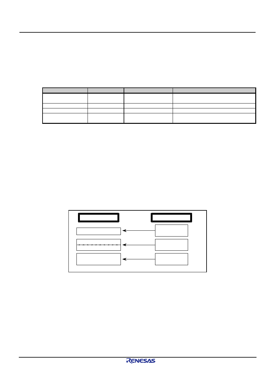
Either a single or double buffer can be selected for PIPE1-5, using the DBLB bit of the PIPExCFG register. The
double buffer is a function that assigns two memory areas specified with the BUFSIZE bit of the PIPEBUF
register to the same pipe. Figure 3.20 shows an example of buffer memory settings for the controller.
64 Byte
128 Byte
BUFSIZE=0,
DBLB=0
BUFIZE=0,
DBLB=1
BUFSIZE=1,
DBLB=0
Buffer memory
PIPEBUF reg
Figure 3.20 Example of buffer memory settings
相关PDF资料 |
PDF描述 |
|---|---|
| M6XXLFXI | OTHER CLOCK GENERATOR, QCC16 |
| M300LFXIT | 50 MHz, OTHER CLOCK GENERATOR, QCC16 |
| M74HC00C1R | HC/UH SERIES, QUAD 2-INPUT NAND GATE, PQCC20 |
| M74HC157B1N | HC/UH SERIES, QUAD 2 LINE TO 1 LINE MULTIPLEXER, TRUE OUTPUT, PDIP16 |
| M74HC158C1 | HC/UH SERIES, QUAD 2 LINE TO 1 LINE MULTIPLEXER, INVERTED OUTPUT, PQCC20 |
相关代理商/技术参数 |
参数描述 |
|---|---|
| M66596WG#RB0Z | 制造商:Renesas Electronics 功能描述:Tray 制造商:Renesas 功能描述:0 |
| M6668 | 制造商:Tamura Corporation of America 功能描述: |
| M66700P | 制造商:MITSUBISHI 制造商全称:Mitsubishi Electric Semiconductor 功能描述:DUAL HIGH-SPEED CCD CLOCK DRIVER |
| M66700WP | 制造商:MITSUBISHI 制造商全称:Mitsubishi Electric Semiconductor 功能描述:DUAL HIGH-SPEED CCD CLOCK DRIVER |
| M66701P | 制造商:MITSUBISHI 制造商全称:Mitsubishi Electric Semiconductor 功能描述:DUAL HIGH-SPEED CCD CLOCK DRIVER |
发布紧急采购,3分钟左右您将得到回复。