- 您现在的位置:买卖IC网 > PDF目录45052 > M66596WG UNIVERSAL SERIAL BUS CONTROLLER, PBGA64 PDF资料下载
参数资料
| 型号: | M66596WG |
| 元件分类: | 总线控制器 |
| 英文描述: | UNIVERSAL SERIAL BUS CONTROLLER, PBGA64 |
| 封装: | 0.80 MM PITCH, FBGA-64 |
| 文件页数: | 65/133页 |
| 文件大小: | 1611K |
| 代理商: | M66596WG |
第1页第2页第3页第4页第5页第6页第7页第8页第9页第10页第11页第12页第13页第14页第15页第16页第17页第18页第19页第20页第21页第22页第23页第24页第25页第26页第27页第28页第29页第30页第31页第32页第33页第34页第35页第36页第37页第38页第39页第40页第41页第42页第43页第44页第45页第46页第47页第48页第49页第50页第51页第52页第53页第54页第55页第56页第57页第58页第59页第60页第61页第62页第63页第64页当前第65页第66页第67页第68页第69页第70页第71页第72页第73页第74页第75页第76页第77页第78页第79页第80页第81页第82页第83页第84页第85页第86页第87页第88页第89页第90页第91页第92页第93页第94页第95页第96页第97页第98页第99页第100页第101页第102页第103页第104页第105页第106页第107页第108页第109页第110页第111页第112页第113页第114页第115页第116页第117页第118页第119页第120页第121页第122页第123页第124页第125页第126页第127页第128页第129页第130页第131页第132页第133页
M66596FP/WG
rev .1.00
2006.3.14
page 35 of 127
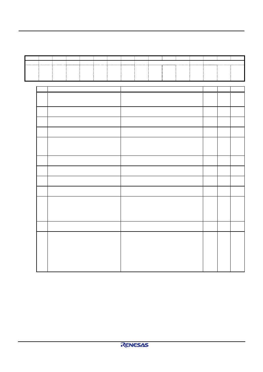
2.9 Interrupt statuses
Interrupt status register 0[INTSTS0]
<Address: 40H>
15
14
13
12
11
10
9
8
7
6
5
4
3
2
1
0
VBINT
RESM
SOFR
DVST
CTRT
BEMP
NRDY
BRDY VBSTS
DVSQ
VALID
CTSQ
0
-
0
-
0
-
0
1
0
-
0
-
0
-
0
-
0
?
-
?
0
1
0
-
0
-
0
-
0
-
0
Bit
Name
Function
S/W
H/W
Note
15 VBINT
VBUS interrupt status
0: VBUS interrupts not issued
1: VBUS interrupts issued
R/W
W
14 RESM
Resume interrupt status
0: Resume interrupts not issued
1: Resume interrupts issued
R/W
W
13 SOFR
Frame number refresh interrupt status
0: SOF interrupts not issued
1: SOF interrupts issued
R/W(0)
W
12 DVST
Device state transition interrupt status
0: Device state transition interrupts not issued
1: Device state transition interrupts issued
R/W(0)
W
11 CTRT
Control transfer stage transition interrupt
status
0: Control transfer stage transition interrupts
not issued
1: Control transfer stage transition interrupts
issued
R/W(0)
W
10 BEMP
Buffer Empty interrupt status
0: BEMP interrupts not issued
1: BEMP interrupts issued
R
W
9
NRDY
Buffer Not Ready interrupt status
0: NRDY interrupts not issued
1: NRDY interrupts issued
R
W
8
BRDY
Buffer Ready interrupt status
0: BRDY interrupts not issued
1: BRDY interrupts issued
R
W
7
VBSTS
VBUS input status
0: VBUS pin is “L” level
1: VBUS pin is “H” level
R
W
6-4 DVSQ
Device state
000: Powered state
001: Default state
010: Address state
011: Configured state
1xx: Suspended state
R
W
3
VALID
Setup packet reception
0: Not detected
1: Setup packet reception
R/W(0)
W
2-0 CTSQ
Control transfer stage
000: Idle or setup stage
001: Control read data stage
010: Control read status stage
011: Control write data stage
100: Control write status stage
101: Control write (NoData) status stage
110: Control transfer sequence error
111: Reserved
R
W
<<Note>>
*1) The BEMP, BRDY and NRDY bits are cleared when all of the factors for each pipe on correcponding registers
have been eliminated, i.e. BEMPSTS, BRDYSTS and NRDYSTS.
*2) The VBUS input status based on the VBSTS bit requires that chattering be eliminated using software.
*3) If multiple factors are being generated among the VBINT, RESM, SOFR, DVST, and CTRT bits, an access cycle
of at least 100 ns is required in order to clear the bits in succession, rather than simultaneously.
相关PDF资料 |
PDF描述 |
|---|---|
| M6XXLFXI | OTHER CLOCK GENERATOR, QCC16 |
| M300LFXIT | 50 MHz, OTHER CLOCK GENERATOR, QCC16 |
| M74HC00C1R | HC/UH SERIES, QUAD 2-INPUT NAND GATE, PQCC20 |
| M74HC157B1N | HC/UH SERIES, QUAD 2 LINE TO 1 LINE MULTIPLEXER, TRUE OUTPUT, PDIP16 |
| M74HC158C1 | HC/UH SERIES, QUAD 2 LINE TO 1 LINE MULTIPLEXER, INVERTED OUTPUT, PQCC20 |
相关代理商/技术参数 |
参数描述 |
|---|---|
| M66596WG#RB0Z | 制造商:Renesas Electronics 功能描述:Tray 制造商:Renesas 功能描述:0 |
| M6668 | 制造商:Tamura Corporation of America 功能描述: |
| M66700P | 制造商:MITSUBISHI 制造商全称:Mitsubishi Electric Semiconductor 功能描述:DUAL HIGH-SPEED CCD CLOCK DRIVER |
| M66700WP | 制造商:MITSUBISHI 制造商全称:Mitsubishi Electric Semiconductor 功能描述:DUAL HIGH-SPEED CCD CLOCK DRIVER |
| M66701P | 制造商:MITSUBISHI 制造商全称:Mitsubishi Electric Semiconductor 功能描述:DUAL HIGH-SPEED CCD CLOCK DRIVER |
发布紧急采购,3分钟左右您将得到回复。