- 您现在的位置:买卖IC网 > PDF目录45052 > M66596WG UNIVERSAL SERIAL BUS CONTROLLER, PBGA64 PDF资料下载
参数资料
| 型号: | M66596WG |
| 元件分类: | 总线控制器 |
| 英文描述: | UNIVERSAL SERIAL BUS CONTROLLER, PBGA64 |
| 封装: | 0.80 MM PITCH, FBGA-64 |
| 文件页数: | 85/133页 |
| 文件大小: | 1611K |
| 代理商: | M66596WG |
第1页第2页第3页第4页第5页第6页第7页第8页第9页第10页第11页第12页第13页第14页第15页第16页第17页第18页第19页第20页第21页第22页第23页第24页第25页第26页第27页第28页第29页第30页第31页第32页第33页第34页第35页第36页第37页第38页第39页第40页第41页第42页第43页第44页第45页第46页第47页第48页第49页第50页第51页第52页第53页第54页第55页第56页第57页第58页第59页第60页第61页第62页第63页第64页第65页第66页第67页第68页第69页第70页第71页第72页第73页第74页第75页第76页第77页第78页第79页第80页第81页第82页第83页第84页当前第85页第86页第87页第88页第89页第90页第91页第92页第93页第94页第95页第96页第97页第98页第99页第100页第101页第102页第103页第104页第105页第106页第107页第108页第109页第110页第111页第112页第113页第114页第115页第116页第117页第118页第119页第120页第121页第122页第123页第124页第125页第126页第127页第128页第129页第130页第131页第132页第133页
M66596FP/WG
rev .1.00
2006.3.14
page 53 of 127
3.1.7.3 Low-power sleep state
The low-power sleep state is set by setting “1” for the PCUT bit of the SYSCFG register. For information on the
sequence in which settings are entered for the low-power sleep state, please refer to Chapter 3.1.8.2 , and for
information on register control timing, please refer to the timing diagram noted later (Figure 3.6 Low-power control
timing diagram).
In the low-power sleep state, of the registers set by software, only registers other than those noted below are
initialized. After returning to the normal operating state, the settings must be re-entered using software. Table 3.5
shows the registers that are not initialized when the controller is in the low-power sleep state.
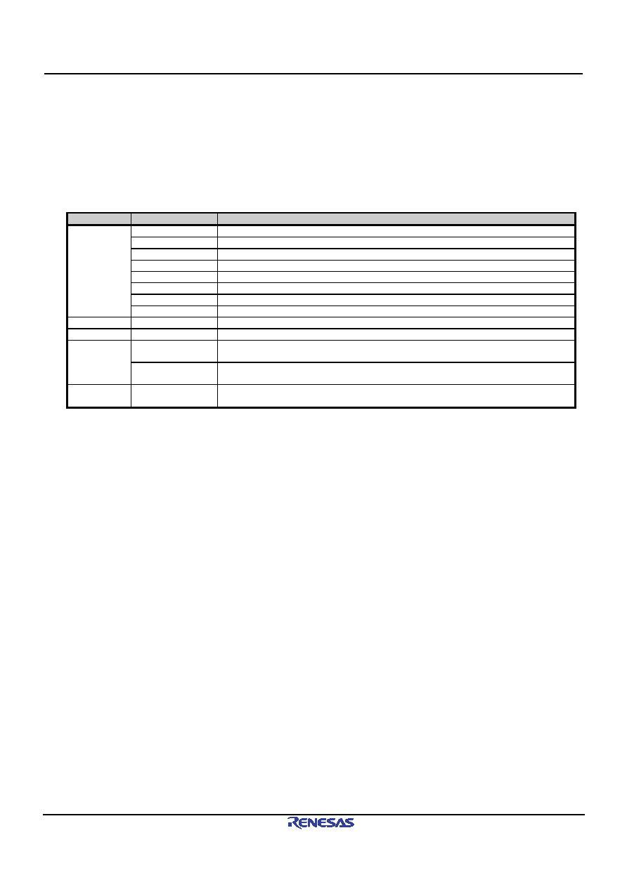
Table 3.5 Registers that are not initialized in the low-power sleep state
Register
Bit
Description
XTAL
This is retained as system information.
ATCKM
This is retained as system information.
HSE
This is retained as system information.
DCFM
This is retained as system information.
DMRPD
This is retained as system information.
DPRPU
This is retained as system information.
FSRPC
This is retained as system information.
SYSCFG
USBE
This is retained as system information.
PINCFG
LDRV
The state of the output pin drive current settings is retained.
DMAxCFG
DREQA
The polarity of the DREQ0_N pin and the DREQ1_N pin are retained.
VBSE / VBINT
When "VBSE=1", if there was any change to the VBUS signal in the low-power
sleep state, the INT_N pin is asserted and notification is made to the CPU.
INTENB0/
INTSTS0
RSME / RESM
When "RSME=1", if there was any change to the USB data bus in the low-power
sleep state, the INT_N pin is asserted and notification is made to the CPU.
INTENB1/
INTSTS1
BCHGE / BCHG
When "BCHGE=1", if there was any change to the USB data bus in the low-power
sleep state, the INT_N pin is asserted and notification is made to the CPU.
相关PDF资料 |
PDF描述 |
|---|---|
| M6XXLFXI | OTHER CLOCK GENERATOR, QCC16 |
| M300LFXIT | 50 MHz, OTHER CLOCK GENERATOR, QCC16 |
| M74HC00C1R | HC/UH SERIES, QUAD 2-INPUT NAND GATE, PQCC20 |
| M74HC157B1N | HC/UH SERIES, QUAD 2 LINE TO 1 LINE MULTIPLEXER, TRUE OUTPUT, PDIP16 |
| M74HC158C1 | HC/UH SERIES, QUAD 2 LINE TO 1 LINE MULTIPLEXER, INVERTED OUTPUT, PQCC20 |
相关代理商/技术参数 |
参数描述 |
|---|---|
| M66596WG#RB0Z | 制造商:Renesas Electronics 功能描述:Tray 制造商:Renesas 功能描述:0 |
| M6668 | 制造商:Tamura Corporation of America 功能描述: |
| M66700P | 制造商:MITSUBISHI 制造商全称:Mitsubishi Electric Semiconductor 功能描述:DUAL HIGH-SPEED CCD CLOCK DRIVER |
| M66700WP | 制造商:MITSUBISHI 制造商全称:Mitsubishi Electric Semiconductor 功能描述:DUAL HIGH-SPEED CCD CLOCK DRIVER |
| M66701P | 制造商:MITSUBISHI 制造商全称:Mitsubishi Electric Semiconductor 功能描述:DUAL HIGH-SPEED CCD CLOCK DRIVER |
发布紧急采购,3分钟左右您将得到回复。