- 您现在的位置:买卖IC网 > PDF目录45052 > M66596WG UNIVERSAL SERIAL BUS CONTROLLER, PBGA64 PDF资料下载
参数资料
| 型号: | M66596WG |
| 元件分类: | 总线控制器 |
| 英文描述: | UNIVERSAL SERIAL BUS CONTROLLER, PBGA64 |
| 封装: | 0.80 MM PITCH, FBGA-64 |
| 文件页数: | 121/133页 |
| 文件大小: | 1611K |
| 代理商: | M66596WG |
第1页第2页第3页第4页第5页第6页第7页第8页第9页第10页第11页第12页第13页第14页第15页第16页第17页第18页第19页第20页第21页第22页第23页第24页第25页第26页第27页第28页第29页第30页第31页第32页第33页第34页第35页第36页第37页第38页第39页第40页第41页第42页第43页第44页第45页第46页第47页第48页第49页第50页第51页第52页第53页第54页第55页第56页第57页第58页第59页第60页第61页第62页第63页第64页第65页第66页第67页第68页第69页第70页第71页第72页第73页第74页第75页第76页第77页第78页第79页第80页第81页第82页第83页第84页第85页第86页第87页第88页第89页第90页第91页第92页第93页第94页第95页第96页第97页第98页第99页第100页第101页第102页第103页第104页第105页第106页第107页第108页第109页第110页第111页第112页第113页第114页第115页第116页第117页第118页第119页第120页当前第121页第122页第123页第124页第125页第126页第127页第128页第129页第130页第131页第132页第133页
M66596FP/WG
rev .1.00
2006.3.14
page 86 of 127
3.5 Data setup timing
This section describes the OBUS bit used to select the timing of split bus.. When there is no description, both a
Host and Peripheral are the same operation.
With this controller, the timing of the SD0-7 and DEND pin can be changed as shown in
Table 3.22, using the OBUS bit
of the DMAxCFG
register The OBUS bit is a function that is valid only for DMA transfers using a split bus. When
using the CPU bus for DMA transfers, the setting of the OBUS bit is ignored.
Table 3.22 Differences in operation based on the value set for the OBUS bit
Direction
OBUS
bit setting
Operation
0
The SD0-7 and DEND signals are output on an ongoing basis, regardless of the control
signal *1)
The next data is output when the control signal is negated.
This assures data setup time for the DMAC and enables high-performance DMA transfers.
Reading
1
The SD0-7 and DEND signals are output after the control signal has been asserted.
The SD0-7 and DEND signals go to the Hi-Z state when the control signal is negated.
0
The SD0-7 and DEND signals can be input on an ongoing basis, regardless of the DACKx_N
signal.
The DMAC can output the next data before the DACKx_N signal is asserted.
This assures data setup time for the controller and enables high-performance DMA transfers.
Writing
1
The SD0-7 and DEND signals can be input only if the DACKx_N signal is asserted.
The SD0-7 and DEND signals are ignored if the DACKx_N signal is negated.
*1) “Control signal” refers to the DACKx_N signal if the DFORM[9-7] of the DMAxCFG register is “100”.
If the DFORM[9-7] is ”110”, it refers to both DACK0_N and DSTRB0_N. In this case, “assertion of the control
signal” means the state in which either DACK0_N or DSTRB0_N is asserted.
If “OBUS=0” is set in the reading direction, the SD0-7 and DEND signals are output on an ongoing basis, so please
be aware that sharing the bus with another device can cause the signals to collide.
If “OBUS=0” is set in the writing direction, the SD0-7 and DEND signals can be input on an ongoing basis, so the
user should make sure that the signals are not set to an intermediate potential.
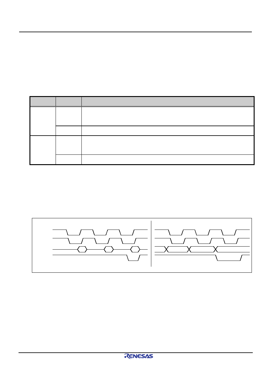
Figure 3.25 shows a schematic diagram of the data setup timing based on the OBUS bit.
OBUS=1: Normal mode
OBUS=0: High-speed mode
DREQ
DACK
SD7-0
DEND
Figure 3.25 Schematic diagram of data setup timing
相关PDF资料 |
PDF描述 |
|---|---|
| M6XXLFXI | OTHER CLOCK GENERATOR, QCC16 |
| M300LFXIT | 50 MHz, OTHER CLOCK GENERATOR, QCC16 |
| M74HC00C1R | HC/UH SERIES, QUAD 2-INPUT NAND GATE, PQCC20 |
| M74HC157B1N | HC/UH SERIES, QUAD 2 LINE TO 1 LINE MULTIPLEXER, TRUE OUTPUT, PDIP16 |
| M74HC158C1 | HC/UH SERIES, QUAD 2 LINE TO 1 LINE MULTIPLEXER, INVERTED OUTPUT, PQCC20 |
相关代理商/技术参数 |
参数描述 |
|---|---|
| M66596WG#RB0Z | 制造商:Renesas Electronics 功能描述:Tray 制造商:Renesas 功能描述:0 |
| M6668 | 制造商:Tamura Corporation of America 功能描述: |
| M66700P | 制造商:MITSUBISHI 制造商全称:Mitsubishi Electric Semiconductor 功能描述:DUAL HIGH-SPEED CCD CLOCK DRIVER |
| M66700WP | 制造商:MITSUBISHI 制造商全称:Mitsubishi Electric Semiconductor 功能描述:DUAL HIGH-SPEED CCD CLOCK DRIVER |
| M66701P | 制造商:MITSUBISHI 制造商全称:Mitsubishi Electric Semiconductor 功能描述:DUAL HIGH-SPEED CCD CLOCK DRIVER |
发布紧急采购,3分钟左右您将得到回复。