- 您现在的位置:买卖IC网 > PDF目录45052 > M66596WG UNIVERSAL SERIAL BUS CONTROLLER, PBGA64 PDF资料下载
参数资料
| 型号: | M66596WG |
| 元件分类: | 总线控制器 |
| 英文描述: | UNIVERSAL SERIAL BUS CONTROLLER, PBGA64 |
| 封装: | 0.80 MM PITCH, FBGA-64 |
| 文件页数: | 118/133页 |
| 文件大小: | 1611K |
| 代理商: | M66596WG |
第1页第2页第3页第4页第5页第6页第7页第8页第9页第10页第11页第12页第13页第14页第15页第16页第17页第18页第19页第20页第21页第22页第23页第24页第25页第26页第27页第28页第29页第30页第31页第32页第33页第34页第35页第36页第37页第38页第39页第40页第41页第42页第43页第44页第45页第46页第47页第48页第49页第50页第51页第52页第53页第54页第55页第56页第57页第58页第59页第60页第61页第62页第63页第64页第65页第66页第67页第68页第69页第70页第71页第72页第73页第74页第75页第76页第77页第78页第79页第80页第81页第82页第83页第84页第85页第86页第87页第88页第89页第90页第91页第92页第93页第94页第95页第96页第97页第98页第99页第100页第101页第102页第103页第104页第105页第106页第107页第108页第109页第110页第111页第112页第113页第114页第115页第116页第117页当前第118页第119页第120页第121页第122页第123页第124页第125页第126页第127页第128页第129页第130页第131页第132页第133页
M66596FP/WG
rev .1.00
2006.3.14
page 83 of 127
3.4.3.3 Zero-Length packet addition mode (DxFIFO port writing direction)
With this controller, it is possible to add and send one Zero-Length packet after all of the data has been sent,
under the conditions noted below, by setting “1” for the DEZPM bit of the DxFIFOSEL register. This function can
be set only if the buffer memory writing direction has been set (a pipe in the sending direction has been set for
the CURPIPE bit).
If the number of data bytes written to the buffer memory is a multiple of the integer for the maximum packet
size when the DEND signal is received
3.4.3.4 DEND pin
The controller is able to terminate DMA transfers that used the DEND pin. The DEND pin has separate input
and output functions, depending on the USB data transfer direction.
(1) Buffer memory reading direction
The DEND pin becomes an output pin, making it possible to notify the external DMA controller of the final
data transfer. The conditions under which the DEND signal is asserted can be set using the PKTM bit of
DMAxCFG
register.
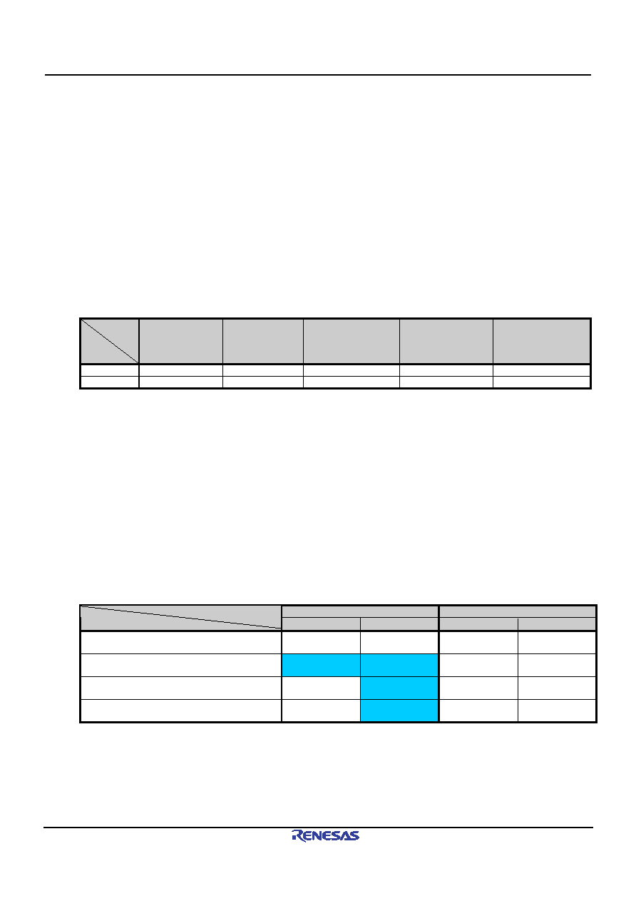
Table 3.19 shows the DEND pin assertion conditions for the controller.
Table 3.19 DEND pin assertions
Event
PKTM
Transaction
count ended
BRDY
generated upon
reception of
packet
Reception of short
packet other than
Zero-Length packet
Reception of
Zero-Length
packet when buffer
is not empty
Reception of
Zero-Length packet
when buffer is
empty
*1
0
Asserted
Not asserted
Asserted
1
Asserted
Not asserted
*1) With reception of a Zero-Length packet when the buffer is empty, the DREQ signal is not asserted.
(2) Buffer memory writing direction
The DEND pin becomes the input pin, and data can be sent from the buffer memory (the same situation as
when “BVAL=1” is set).
3.4.3.5 DxFIFO auto clear mode (DxFIFO port reading direction)
If “1” is set for the DCLRM bit of the DxFIFOSEL register, the controller automatically clears the buffer
memory of the pertinent pipe when reading of the data from the buffer memory has been completed.
Table 3.20 shows the packet reception and buffer memory clearing processing for each of the various settings.
Using the DCLRM bit eliminates the need for the buffer to be cleared by software even if a situation occurs
that necessitates clearing of the buffer. This makes it possible to carry out DMA transfers without involving the
control program. This function can be set only in the buffer memory reading direction.
Table 3.20 Packet reception and buffer memory clearing processing
DCLRM = “0”
DCLRM = “1”
Register setting
Buffer status when packet is received
BFRE=0
BFRE=1
BFRE=0
BFRE=1
Buffer full
Doesn’t need to
be cleared
Doesn’t need to
be cleared
Doesn’t need to
be cleared
Doesn’t need to
be cleared
Zero-Length packet reception
Needs to be
cleared
Needs to be
cleared
Doesn’t need to
be cleared
Doesn’t need to
be cleared
Normal short packet reception
Doesn’t need to
be cleared
Needs to be
cleared
Doesn’t need to
be cleared
Doesn’t need to
be cleared
Transaction count ended
Doesn’t need to
be cleared
Needs to be
cleared
Doesn’t need to
be cleared
Doesn’t need to
be cleared
相关PDF资料 |
PDF描述 |
|---|---|
| M6XXLFXI | OTHER CLOCK GENERATOR, QCC16 |
| M300LFXIT | 50 MHz, OTHER CLOCK GENERATOR, QCC16 |
| M74HC00C1R | HC/UH SERIES, QUAD 2-INPUT NAND GATE, PQCC20 |
| M74HC157B1N | HC/UH SERIES, QUAD 2 LINE TO 1 LINE MULTIPLEXER, TRUE OUTPUT, PDIP16 |
| M74HC158C1 | HC/UH SERIES, QUAD 2 LINE TO 1 LINE MULTIPLEXER, INVERTED OUTPUT, PQCC20 |
相关代理商/技术参数 |
参数描述 |
|---|---|
| M66596WG#RB0Z | 制造商:Renesas Electronics 功能描述:Tray 制造商:Renesas 功能描述:0 |
| M6668 | 制造商:Tamura Corporation of America 功能描述: |
| M66700P | 制造商:MITSUBISHI 制造商全称:Mitsubishi Electric Semiconductor 功能描述:DUAL HIGH-SPEED CCD CLOCK DRIVER |
| M66700WP | 制造商:MITSUBISHI 制造商全称:Mitsubishi Electric Semiconductor 功能描述:DUAL HIGH-SPEED CCD CLOCK DRIVER |
| M66701P | 制造商:MITSUBISHI 制造商全称:Mitsubishi Electric Semiconductor 功能描述:DUAL HIGH-SPEED CCD CLOCK DRIVER |
发布紧急采购,3分钟左右您将得到回复。