- 您现在的位置:买卖IC网 > PDF目录45052 > M66596WG UNIVERSAL SERIAL BUS CONTROLLER, PBGA64 PDF资料下载
参数资料
| 型号: | M66596WG |
| 元件分类: | 总线控制器 |
| 英文描述: | UNIVERSAL SERIAL BUS CONTROLLER, PBGA64 |
| 封装: | 0.80 MM PITCH, FBGA-64 |
| 文件页数: | 53/133页 |
| 文件大小: | 1611K |
| 代理商: | M66596WG |
第1页第2页第3页第4页第5页第6页第7页第8页第9页第10页第11页第12页第13页第14页第15页第16页第17页第18页第19页第20页第21页第22页第23页第24页第25页第26页第27页第28页第29页第30页第31页第32页第33页第34页第35页第36页第37页第38页第39页第40页第41页第42页第43页第44页第45页第46页第47页第48页第49页第50页第51页第52页当前第53页第54页第55页第56页第57页第58页第59页第60页第61页第62页第63页第64页第65页第66页第67页第68页第69页第70页第71页第72页第73页第74页第75页第76页第77页第78页第79页第80页第81页第82页第83页第84页第85页第86页第87页第88页第89页第90页第91页第92页第93页第94页第95页第96页第97页第98页第99页第100页第101页第102页第103页第104页第105页第106页第107页第108页第109页第110页第111页第112页第113页第114页第115页第116页第117页第118页第119页第120页第121页第122页第123页第124页第125页第126页第127页第128页第129页第130页第131页第132页第133页
M66596FP/WG
rev .1.00
2006.3.14
page 24 of 127
The DMA0CFG register controls the input/output pins used for the DMA0 interface and the D0FIFO port, and the
DMA1CFG
register controls the input/output pins used for the DMA1 interface and the D1FIFO port.
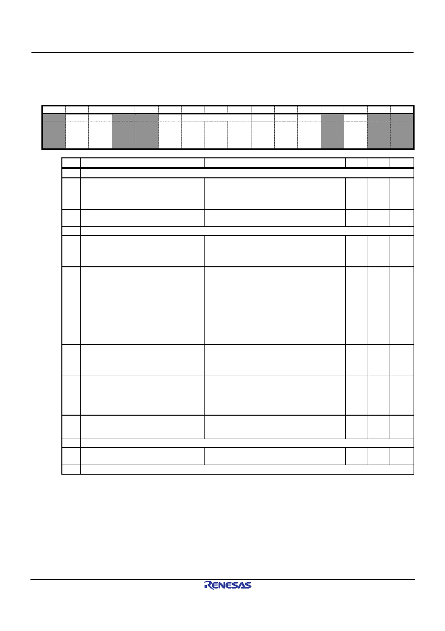
DMA0 pin configuration register [DMA0CFG]
<Address: 0CH>
DMA1 pin configuration register [DMA1CFG]
<Address: 0EH>
15
14
13
12
11
10
9
8
7
6
5
4
3
2
1
0
DREQA BURST
DACKA
DFORM
DENDA PKTM DENDE
OBUS
?
0
-
0
-
0
?
0
-
0
-
0
-
0
-
0
-
0
-
0
-
0
?
0
-
0
?
Bit
Name
Function
S/W
H/W
Note
15 Nothing is placed here. This should be fixed at “0”.
14 DREQA
DREQx_N signal polarity selection
This specifies the active state for the DREQx_N
pin.
0: Low active
1: High active
R/W
R
-
13 BURST
Burst mode
0: Cycle steal transfer
1: Burst transfer
R/W
R
12-11 Nothing is placed here. These should be fixed at “0”.
10 DACKA
DACKx_N signal polarity selection
This specifies the active state for the DACKx_N
pin.
0: Low active
1: High active
R/W
R
-
9-7 DFORM
DMA transfer signal selection
011:
Only the DACKx_N signal is used (CPU
bus).
000:
The Address signal + the RD_N/WRx_
signals are used (CPU bus).
010:
The DACKx_N + the RD_N/WRx_N
signals are used (CPU bus).
100:
The DACKx_N signal is used (split bus).
110:
The DACK0_N + the DSTB0_N signal
are used (split bus).
001, 101, 111: Reserved
R/W
R
6
DENDA
DEND0_N signal polarity selection
This specifies the active state of the DENDx_N
pin.
0: Low active
1: High active
R/W
R
-
5
PKTM
Packet mode
0: The DENDx_N signal is asserted in transfer
units.
1: The DENDx_N signal is asserted each time
an amount of data corresponding to the buffer
size is transferred.
R/W
R
4
DENDE
DENDx_N signal enabled
0: The DENDx_N signal is disabled
(Hi-Z output).
1: The DENDx_N signal is enabled.
R/W
R
3
Nothing is placed here. It should be fixed at “0”.
2
OBUS
OBUS operation
disabled
0: The OBUS mode is enabled.
1: The OBUS mode is disabled.
R/W
R
1-0 Nothing is placed here. These should be fixed at "0”.
<<Notes>>
*2) The PKTM bit is valid only when the data receiving direction (reading from the buffer memory) is set. If the
DxFIFO port is being used in the data writing direction, “PKTM=0” should be set.
*3) The “DFORM=110” setting is valid only when the DMA channel 0 is set.
Also, the following should not be set: "DFORM=001”,"DFORM=101” and"DFORM=111”.
相关PDF资料 |
PDF描述 |
|---|---|
| M6XXLFXI | OTHER CLOCK GENERATOR, QCC16 |
| M300LFXIT | 50 MHz, OTHER CLOCK GENERATOR, QCC16 |
| M74HC00C1R | HC/UH SERIES, QUAD 2-INPUT NAND GATE, PQCC20 |
| M74HC157B1N | HC/UH SERIES, QUAD 2 LINE TO 1 LINE MULTIPLEXER, TRUE OUTPUT, PDIP16 |
| M74HC158C1 | HC/UH SERIES, QUAD 2 LINE TO 1 LINE MULTIPLEXER, INVERTED OUTPUT, PQCC20 |
相关代理商/技术参数 |
参数描述 |
|---|---|
| M66596WG#RB0Z | 制造商:Renesas Electronics 功能描述:Tray 制造商:Renesas 功能描述:0 |
| M6668 | 制造商:Tamura Corporation of America 功能描述: |
| M66700P | 制造商:MITSUBISHI 制造商全称:Mitsubishi Electric Semiconductor 功能描述:DUAL HIGH-SPEED CCD CLOCK DRIVER |
| M66700WP | 制造商:MITSUBISHI 制造商全称:Mitsubishi Electric Semiconductor 功能描述:DUAL HIGH-SPEED CCD CLOCK DRIVER |
| M66701P | 制造商:MITSUBISHI 制造商全称:Mitsubishi Electric Semiconductor 功能描述:DUAL HIGH-SPEED CCD CLOCK DRIVER |
发布紧急采购,3分钟左右您将得到回复。