- 您现在的位置:买卖IC网 > PDF目录136617 > S1C17554B00E10L 16-BIT, FLASH, 24 MHz, RISC MICROCONTROLLER, PBGA48 PDF资料下载
参数资料
| 型号: | S1C17554B00E10L |
| 元件分类: | 微控制器/微处理器 |
| 英文描述: | 16-BIT, FLASH, 24 MHz, RISC MICROCONTROLLER, PBGA48 |
| 封装: | 3.137 X 3.137 MM, 0.72 MM HEIGHT, 0.40 MM PITCH, WCSP-48 |
| 文件页数: | 207/318页 |
| 文件大小: | 2643K |
| 代理商: | S1C17554B00E10L |
第1页第2页第3页第4页第5页第6页第7页第8页第9页第10页第11页第12页第13页第14页第15页第16页第17页第18页第19页第20页第21页第22页第23页第24页第25页第26页第27页第28页第29页第30页第31页第32页第33页第34页第35页第36页第37页第38页第39页第40页第41页第42页第43页第44页第45页第46页第47页第48页第49页第50页第51页第52页第53页第54页第55页第56页第57页第58页第59页第60页第61页第62页第63页第64页第65页第66页第67页第68页第69页第70页第71页第72页第73页第74页第75页第76页第77页第78页第79页第80页第81页第82页第83页第84页第85页第86页第87页第88页第89页第90页第91页第92页第93页第94页第95页第96页第97页第98页第99页第100页第101页第102页第103页第104页第105页第106页第107页第108页第109页第110页第111页第112页第113页第114页第115页第116页第117页第118页第119页第120页第121页第122页第123页第124页第125页第126页第127页第128页第129页第130页第131页第132页第133页第134页第135页第136页第137页第138页第139页第140页第141页第142页第143页第144页第145页第146页第147页第148页第149页第150页第151页第152页第153页第154页第155页第156页第157页第158页第159页第160页第161页第162页第163页第164页第165页第166页第167页第168页第169页第170页第171页第172页第173页第174页第175页第176页第177页第178页第179页第180页第181页第182页第183页第184页第185页第186页第187页第188页第189页第190页第191页第192页第193页第194页第195页第196页第197页第198页第199页第200页第201页第202页第203页第204页第205页第206页当前第207页第208页第209页第210页第211页第212页第213页第214页第215页第216页第217页第218页第219页第220页第221页第222页第223页第224页第225页第226页第227页第228页第229页第230页第231页第232页第233页第234页第235页第236页第237页第238页第239页第240页第241页第242页第243页第244页第245页第246页第247页第248页第249页第250页第251页第252页第253页第254页第255页第256页第257页第258页第259页第260页第261页第262页第263页第264页第265页第266页第267页第268页第269页第270页第271页第272页第273页第274页第275页第276页第277页第278页第279页第280页第281页第282页第283页第284页第285页第286页第287页第288页第289页第290页第291页第292页第293页第294页第295页第296页第297页第298页第299页第300页第301页第302页第303页第304页第305页第306页第307页第308页第309页第310页第311页第312页第313页第314页第315页第316页第317页第318页
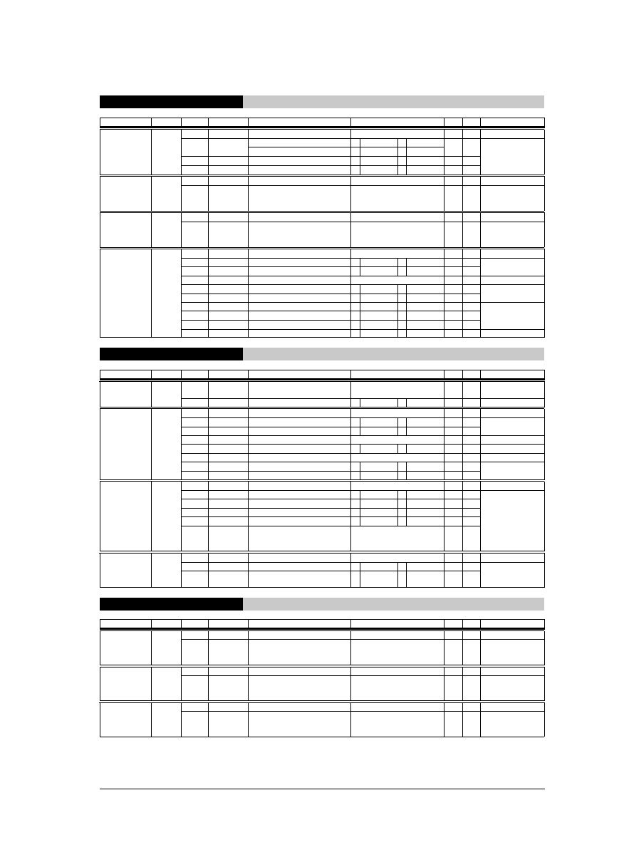
APPENDIX A LIST OF I/O REGISTERS
S1C17554/564 TECHNICAL MANUAL
Seiko Epson Corporation
AP-A-11
0x4320–0x4326
SPI Ch.0
Register name Address
Bit
Name
Function
Setting
Init. R/W
Remarks
SPI Ch.0
Status Register
(SPI_ST0)
0x4320
(16 bits)
D15–3 –
reserved
–
0 when being read.
D2
SPBSY
Transfer busy flag (master)
1 Busy
0 Idle
0
R
ss signal low flag (slave)
1 ss = L
0 ss = H
D1
SPRBF
Receive data buffer full flag
1 Full
0 Not full
0
R
D0
SPTBE
Transmit data buffer empty flag
1 Empty
0 Not empty
1
R
SPI Ch.0
Transmit Data
Register
(SPI_TXD0)
0x4322
(16 bits)
D15–8 –
reserved
–
0 when being read.
D7–0 SPTDB[7:0] SPI transmit data buffer
SPTDB7 = MSB
SPTDB0 = LSB
0x0 to 0xff
0x0 R/W
SPI Ch.0
Receive Data
Register
(SPI_RXD0)
0x4324
(16 bits)
D15–8 –
reserved
–
0 when being read.
D7–0 SPRDB[7:0] SPI receive data buffer
SPRDB7 = MSB
SPRDB0 = LSB
0x0 to 0xff
0x0
R
SPI Ch.0
Control Register
(SPI_CTL0)
0x4326
(16 bits)
D15–10 –
reserved
–
0 when being read.
D9
MCLK
SPI clock source select
1 T16 Ch.1
0 PCLK/4
0
R/W
D8
MLSB
LSB/MSB first mode select
1 LSB
0 MSB
0
R/W
D7–6 –
reserved
–
0 when being read.
D5
SPRIE
Receive data buffer full int. enable 1 Enable
0 Disable
0
R/W
D4
SPTIE
Transmit data buffer empty int. enable 1 Enable
0 Disable
0
R/W
D3
CPHA
Clock phase select
1 Data out
0 Data in
0
R/W These bits must be
set before setting
SPEN to 1.
D2
CPOL
Clock polarity select
1 Active L
0 Active H
0
R/W
D1
MSSL
Master/slave mode select
1 Master
0 Slave
0
R/W
D0
SPEN
SPI enable
1 Enable
0 Disable
0
R/W
0x4340–0x4346
I2C Master
Register name Address
Bit
Name
Function
Setting
Init. R/W
Remarks
I2C Master
Enable Register
(I2CM_EN)
0x4340
(16 bits)
D15–1 –
reserved
–
0 when being read.
D0
I2CMEN
I2C master enable
1 Enable
0 Disable
0
R/W
I2C Master
Control Register
(I2CM_CTL)
0x4342
(16 bits)
D15–10 –
reserved
–
0 when being read.
D9
RBUSY
Receive busy flag
1 Busy
0 Idle
0
R
D8
TBUSY
Transmit busy flag
1 Busy
0 Idle
0
R
D7–5 –
reserved
–
0 when being read.
D4
NSERM
Noise remove on/off
1 On
0 Off
0
R/W
D3–2 –
reserved
–
0 when being read.
D1
STP
Stop control
1 Stop
0 Ignored
0
R/W
D0
STRT
Start control
1 Start
0 Ignored
0
R/W
I2C Master
Data Register
(I2CM_DAT)
0x4344
(16 bits)
D15–12 –
reserved
–
0 when being read.
D11
RBRDY
Receive buffer ready flag
1 Ready
0 Empty
0
R
D10
RXE
Receive execution
1 Receive
0 Ignored
0
R/W
D9
TXE
Transmit execution
1 Transmit
0 Ignored
0
R/W
D8
RTACK
Receive/transmit ACK
1 Error
0 ACK
0
R/W
D7–0 RTDT[7:0]
Receive/transmit data
RTDT7 = MSB
RTDT0 = LSB
0x0 to 0xff
0x0 R/W
I2C Master
Interrupt
Control Register
(I2CM_ICTL)
0x4346
(16 bits)
D15–2 –
reserved
–
0 when being read.
D1
RINTE
Receive interrupt enable
1 Enable
0 Disable
0
R/W
D0
TINTE
Transmit interrupt enable
1 Enable
0 Disable
0
R/W
0x4360–0x436c
I2C Slave
Register name Address
Bit
Name
Function
Setting
Init. R/W
Remarks
I2C Slave
Transmit Data
Register
(I2CS_TRNS)
0x4360
(16 bits)
D15–8 –
reserved
–
0 when being read.
D7–0 SDATA[7:0] I2C slave transmit data
0–0xff
0x0 R/W
I2C Slave
Receive Data
Register
(I2CS_RECV)
0x4362
(16 bits)
D15–8 –
reserved
–
0 when being read.
D7–0 RDATA[7:0] I2C slave receive data
0–0xff
0x0
R
I2C Slave
Address Setup
Register
(I2CS_SADRS)
0x4364
(16 bits)
D15–7 –
reserved
–
0 when being read.
D6–0 SADRS[6:0] I2C slave address
0–0x7f
0x0 R/W
相关PDF资料 |
PDF描述 |
|---|---|
| S1C17554D00E10H | 16-BIT, FLASH, 24 MHz, RISC MICROCONTROLLER, UUC |
| S1C17554F00E10P | 16-BIT, FLASH, 24 MHz, RISC MICROCONTROLLER, PQFP64 |
| S1C17564D00E199 | 16-BIT, FLASH, 24 MHz, RISC MICROCONTROLLER, UUC |
| S1C17651B00E199 | 16-BIT, FLASH, 2 MHz, RISC MICROCONTROLLER, PBGA |
| SPC563M54L3COBR | 32-BIT, FLASH, 64 MHz, MICROCONTROLLER, PQFP100 |
相关代理商/技术参数 |
参数描述 |
|---|---|
| S1C17555 | 制造商:EPSON 制造商全称:EPSON 功能描述:16-bit Single Chip Microcontroller |
| S1C17564 | 制造商:EPSON 制造商全称:EPSON 功能描述:16-bit Single Chip Microcontroller |
| S1C17564D111000 | 制造商:Epson Electronics America Inc 功能描述:16-bit, 128KB Flash (OSC3 = Ceramic) |
| S1C17564F111100 | 功能描述:显示驱动器和控制器 16-bit, 128KB Flash RoHS:否 制造商:Panasonic Electronic Components 工作电源电压:2.7 V to 5.5 V 最大工作温度: 安装风格:SMD/SMT 封装 / 箱体:QFN-44 封装:Reel |
| S1C17565 | 制造商:EPSON 制造商全称:EPSON 功能描述:16-bit Single Chip Microcontroller |
发布紧急采购,3分钟左右您将得到回复。