- 您现在的位置:买卖IC网 > PDF目录136617 > S1C17554B00E10L 16-BIT, FLASH, 24 MHz, RISC MICROCONTROLLER, PBGA48 PDF资料下载
参数资料
| 型号: | S1C17554B00E10L |
| 元件分类: | 微控制器/微处理器 |
| 英文描述: | 16-BIT, FLASH, 24 MHz, RISC MICROCONTROLLER, PBGA48 |
| 封装: | 3.137 X 3.137 MM, 0.72 MM HEIGHT, 0.40 MM PITCH, WCSP-48 |
| 文件页数: | 238/318页 |
| 文件大小: | 2643K |
| 代理商: | S1C17554B00E10L |
第1页第2页第3页第4页第5页第6页第7页第8页第9页第10页第11页第12页第13页第14页第15页第16页第17页第18页第19页第20页第21页第22页第23页第24页第25页第26页第27页第28页第29页第30页第31页第32页第33页第34页第35页第36页第37页第38页第39页第40页第41页第42页第43页第44页第45页第46页第47页第48页第49页第50页第51页第52页第53页第54页第55页第56页第57页第58页第59页第60页第61页第62页第63页第64页第65页第66页第67页第68页第69页第70页第71页第72页第73页第74页第75页第76页第77页第78页第79页第80页第81页第82页第83页第84页第85页第86页第87页第88页第89页第90页第91页第92页第93页第94页第95页第96页第97页第98页第99页第100页第101页第102页第103页第104页第105页第106页第107页第108页第109页第110页第111页第112页第113页第114页第115页第116页第117页第118页第119页第120页第121页第122页第123页第124页第125页第126页第127页第128页第129页第130页第131页第132页第133页第134页第135页第136页第137页第138页第139页第140页第141页第142页第143页第144页第145页第146页第147页第148页第149页第150页第151页第152页第153页第154页第155页第156页第157页第158页第159页第160页第161页第162页第163页第164页第165页第166页第167页第168页第169页第170页第171页第172页第173页第174页第175页第176页第177页第178页第179页第180页第181页第182页第183页第184页第185页第186页第187页第188页第189页第190页第191页第192页第193页第194页第195页第196页第197页第198页第199页第200页第201页第202页第203页第204页第205页第206页第207页第208页第209页第210页第211页第212页第213页第214页第215页第216页第217页第218页第219页第220页第221页第222页第223页第224页第225页第226页第227页第228页第229页第230页第231页第232页第233页第234页第235页第236页第237页当前第238页第239页第240页第241页第242页第243页第244页第245页第246页第247页第248页第249页第250页第251页第252页第253页第254页第255页第256页第257页第258页第259页第260页第261页第262页第263页第264页第265页第266页第267页第268页第269页第270页第271页第272页第273页第274页第275页第276页第277页第278页第279页第280页第281页第282页第283页第284页第285页第286页第287页第288页第289页第290页第291页第292页第293页第294页第295页第296页第297页第298页第299页第300页第301页第302页第303页第304页第305页第306页第307页第308页第309页第310页第311页第312页第313页第314页第315页第316页第317页第318页
APPENDIX C MOUNTING PRECAUTIONS
AP-C-2
Seiko Epson Corporation
S1C17554/564 TECHNICAL MANUAL
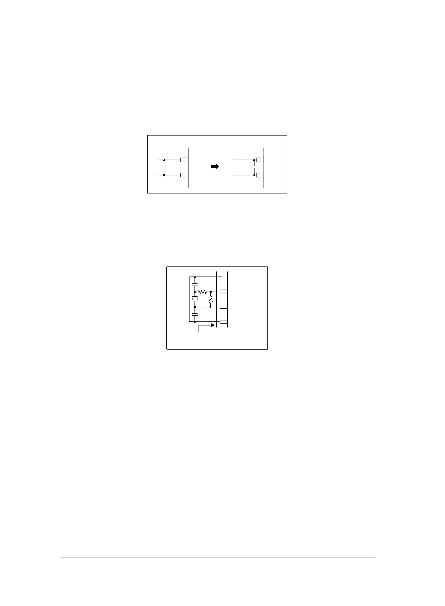
Power supply circuit
Sudden power supply fluctuations due to noise will cause malfunctions. Consider the following issues.
(1) Connections from the power supply to the
*VDD (LVDD, HVDD, AVDD) and VSS pins should be implement-
ed via the shortest, thickest patterns possible.
(2) If a bypass capacitor is connected between
*VDD and VSS, connections between the *VDD and VSS pins
should be as short as possible.
*VDD
VSS
Bypass capacitor connection example
*VDD
VSS
Signal line location
To prevent electromagnetically-induced noise arising from mutual induction, large-current signal lines should
not be positioned close to circuits susceptible to noise, such as oscillators.
Locating signal lines in parallel over significant distances or crossing signal lines operating at high speed will
cause malfunctions due to noise generated by mutual interference. Specifically, avoid positioning crossing
signal lines operating at high speed close to circuits susceptible to noise, such as oscillators.
OSC1, OSC3
OSC2, OSC4
VSS
Large current signal line
High-speed signal line
Prohibited pattern
Noise-induced malfunctions
Check the following three points if you suspect the presence of noise-induced IC malfunctions.
(1) DSIO pin
Low-level noise to this pin will cause a switch to debug mode. The switch to debug mode can be confirmed
by the clock output from DCLK and a High signal from the DST2 pin.
For the product version, we recommend connecting the DSIO pin directly to HVDD or pulling up the DISO
pin using a resistor not exceeding 10 k
W. The IC includes an internal pull-up resistor. The resistor has a
relatively high impedance of 100 k
W to 500 kW and is not noise-resistant.
(2) #RESET pin
Low-level noise to this pin will reset the IC. Depending on the input waveform, the reset may not proceed
correctly. This is more likely to occur if, due to circuit design choices, the impedance is high when the reset
input is High.
(3) LVDD, HVDD, AVDD, and VSS power supply
The IC will malfunction at the instant when noise falling below the rated voltage is input. Incorporate coun-
termeasures on the circuit board, including close patterns for circuit board power supply circuits, noise-
filtering decoupling capacitors, and surge/noise prevention components on the power supply line.
Perform the inspections described above using an oscilloscope capable of observing waveforms of at least 200
MHz. It may not be possible to observe high-speed noise events with a low-speed oscilloscope.
相关PDF资料 |
PDF描述 |
|---|---|
| S1C17554D00E10H | 16-BIT, FLASH, 24 MHz, RISC MICROCONTROLLER, UUC |
| S1C17554F00E10P | 16-BIT, FLASH, 24 MHz, RISC MICROCONTROLLER, PQFP64 |
| S1C17564D00E199 | 16-BIT, FLASH, 24 MHz, RISC MICROCONTROLLER, UUC |
| S1C17651B00E199 | 16-BIT, FLASH, 2 MHz, RISC MICROCONTROLLER, PBGA |
| SPC563M54L3COBR | 32-BIT, FLASH, 64 MHz, MICROCONTROLLER, PQFP100 |
相关代理商/技术参数 |
参数描述 |
|---|---|
| S1C17555 | 制造商:EPSON 制造商全称:EPSON 功能描述:16-bit Single Chip Microcontroller |
| S1C17564 | 制造商:EPSON 制造商全称:EPSON 功能描述:16-bit Single Chip Microcontroller |
| S1C17564D111000 | 制造商:Epson Electronics America Inc 功能描述:16-bit, 128KB Flash (OSC3 = Ceramic) |
| S1C17564F111100 | 功能描述:显示驱动器和控制器 16-bit, 128KB Flash RoHS:否 制造商:Panasonic Electronic Components 工作电源电压:2.7 V to 5.5 V 最大工作温度: 安装风格:SMD/SMT 封装 / 箱体:QFN-44 封装:Reel |
| S1C17565 | 制造商:EPSON 制造商全称:EPSON 功能描述:16-bit Single Chip Microcontroller |
发布紧急采购,3分钟左右您将得到回复。