- 您现在的位置:买卖IC网 > PDF目录298840 > AU1550500MBC (ADVANCED MICRO DEVICES INC) 500 MHz, MICROPROCESSOR, PBGA483 PDF资料下载
参数资料
| 型号: | AU1550500MBC |
| 厂商: | ADVANCED MICRO DEVICES INC |
| 元件分类: | 微控制器/微处理器 |
| 英文描述: | 500 MHz, MICROPROCESSOR, PBGA483 |
| 封装: | 21 X 21 MM, 0.80 MM PITCH, PLASTIC, LBGA-483 |
| 文件页数: | 331/468页 |
| 文件大小: | 3308K |
| 代理商: | AU1550500MBC |
第1页第2页第3页第4页第5页第6页第7页第8页第9页第10页第11页第12页第13页第14页第15页第16页第17页第18页第19页第20页第21页第22页第23页第24页第25页第26页第27页第28页第29页第30页第31页第32页第33页第34页第35页第36页第37页第38页第39页第40页第41页第42页第43页第44页第45页第46页第47页第48页第49页第50页第51页第52页第53页第54页第55页第56页第57页第58页第59页第60页第61页第62页第63页第64页第65页第66页第67页第68页第69页第70页第71页第72页第73页第74页第75页第76页第77页第78页第79页第80页第81页第82页第83页第84页第85页第86页第87页第88页第89页第90页第91页第92页第93页第94页第95页第96页第97页第98页第99页第100页第101页第102页第103页第104页第105页第106页第107页第108页第109页第110页第111页第112页第113页第114页第115页第116页第117页第118页第119页第120页第121页第122页第123页第124页第125页第126页第127页第128页第129页第130页第131页第132页第133页第134页第135页第136页第137页第138页第139页第140页第141页第142页第143页第144页第145页第146页第147页第148页第149页第150页第151页第152页第153页第154页第155页第156页第157页第158页第159页第160页第161页第162页第163页第164页第165页第166页第167页第168页第169页第170页第171页第172页第173页第174页第175页第176页第177页第178页第179页第180页第181页第182页第183页第184页第185页第186页第187页第188页第189页第190页第191页第192页第193页第194页第195页第196页第197页第198页第199页第200页第201页第202页第203页第204页第205页第206页第207页第208页第209页第210页第211页第212页第213页第214页第215页第216页第217页第218页第219页第220页第221页第222页第223页第224页第225页第226页第227页第228页第229页第230页第231页第232页第233页第234页第235页第236页第237页第238页第239页第240页第241页第242页第243页第244页第245页第246页第247页第248页第249页第250页第251页第252页第253页第254页第255页第256页第257页第258页第259页第260页第261页第262页第263页第264页第265页第266页第267页第268页第269页第270页第271页第272页第273页第274页第275页第276页第277页第278页第279页第280页第281页第282页第283页第284页第285页第286页第287页第288页第289页第290页第291页第292页第293页第294页第295页第296页第297页第298页第299页第300页第301页第302页第303页第304页第305页第306页第307页第308页第309页第310页第311页第312页第313页第314页第315页第316页第317页第318页第319页第320页第321页第322页第323页第324页第325页第326页第327页第328页第329页第330页当前第331页第332页第333页第334页第335页第336页第337页第338页第339页第340页第341页第342页第343页第344页第345页第346页第347页第348页第349页第350页第351页第352页第353页第354页第355页第356页第357页第358页第359页第360页第361页第362页第363页第364页第365页第366页第367页第368页第369页第370页第371页第372页第373页第374页第375页第376页第377页第378页第379页第380页第381页第382页第383页第384页第385页第386页第387页第388页第389页第390页第391页第392页第393页第394页第395页第396页第397页第398页第399页第400页第401页第402页第403页第404页第405页第406页第407页第408页第409页第410页第411页第412页第413页第414页第415页第416页第417页第418页第419页第420页第421页第422页第423页第424页第425页第426页第427页第428页第429页第430页第431页第432页第433页第434页第435页第436页第437页第438页第439页第440页第441页第442页第443页第444页第445页第446页第447页第448页第449页第450页第451页第452页第453页第454页第455页第456页第457页第458页第459页第460页第461页第462页第463页第464页第465页第466页第467页第468页
AMD Alchemy Au1550 Security Network Processor Data Book
397
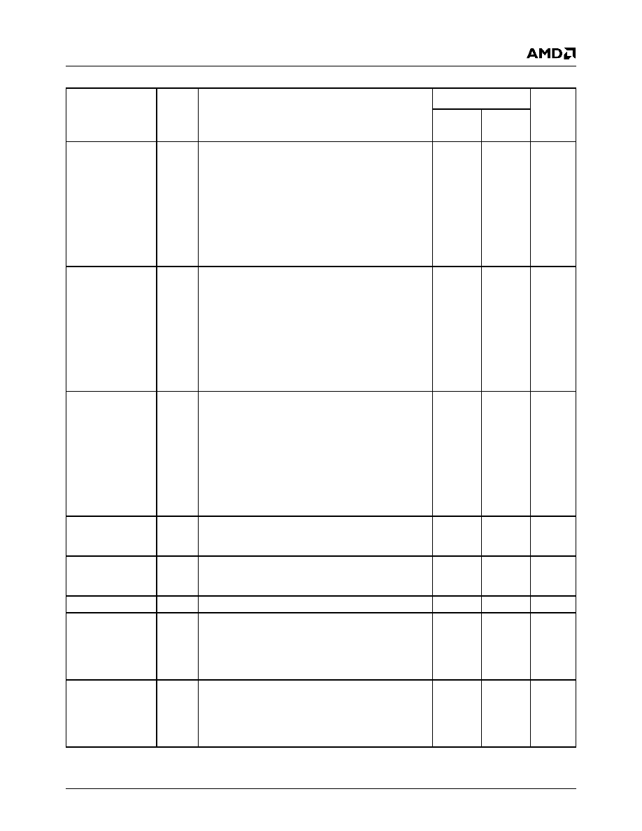
Signal Descriptions
30283D
GPIO[10]
IOZ
General Purpose I/O. Muxed with U3DSR#. GPIO[10]
is the default signal coming out of hardware reset,
runtime reset, and Sleep.
Note:
For systems that use the UART3 interface
without the optional modem control signals
(sys_pinfunc[UR3]=0), the modem status
interrupts
must
be
disabled
(uart3_inten[MIE]=0) to avoid false UART3
interrupts when using GPIO[9], GPIO[10],
GPIO[11], or GPIO[12] as an input.
HIZ
LV
GPIO[11]
IOZ
General Purpose I/O. Muxed with U3DCD#. GPIO[11]
is the default signal coming out of hardware reset,
runtime reset, and Sleep.
Note:
For systems that use the UART3 interface
without the optional modem control signals
(sys_pinfunc[UR3]=0), the modem status
interrupts
must
be
disabled
(uart3_inten[MIE]=0) to avoid false UART3
interrupts when using GPIO[9], GPIO[10],
GPIO[11], or GPIO[12] as an input.
HIZ
LV
GPIO[12]
IOZ
General Purpose I/O. Muxed with U3RI#. GPIO[12] is
the default signal coming out of hardware reset, runt-
ime reset, and Sleep.
Note:
For systems that use the UART3 interface
without the optional modem control signals
(sys_pinfunc[UR3]=0), the modem status
interrupts
must
be
disabled
(uart3_inten[MIE]=0) to avoid false UART3
interrupts when using GPIO[9], GPIO[10],
GPIO[11], or GPIO[12] as an input.
HIZ
LV
GPIO[13]
IOZ
General Purpose I/O. Muxed with U3RTS#. GPIO[13]
is the default signal coming out of hardware reset,
runtime reset, and Sleep.
HIZ
LV
GPIO[14]
IOZ
General Purpose I/O. Muxed with U3DTR#. GPIO[14]
is the default signal coming out of hardware reset,
runtime reset, and Sleep.
HIZ
LV
GPIO[15]
IOZ
General Purpose I/O.
HIZ
LV
GPIO[16]
IOZ
General Purpose I/O. Muxed with PSC0_SYNC1.
PSC0_SYNC1 is the default signal coming out of
hardware reset, runtime reset, and Sleep.
Note:
The GPIO[16]/PSC0_SYNC1 pin is driven
high coming out of reset.
NA
LV
GPIO[17]
IOZ
General Purpose I/O. Muxed with PSC1_SYNC1.
PSC1_SYNC1 is the default signal coming out of
hardware reset, runtime reset, and Sleep.
Note:
The GPIO[17]/PSC1_SYNC1 pin is driven
high coming out of reset.
NA
LV
Table 13-3. External Signals (Continued)
Signal
Type
Description
Reset
During
Sleep
HW
Run
Time
相关PDF资料 |
PDF描述 |
|---|---|
| AU1PDHM3/84A | 1 A, 200 V, SILICON, SIGNAL DIODE, DO-220AA |
| AUM005A0D-SRZ | 1-OUTPUT 10 W DC-DC REG PWR SUPPLY MODULE |
| AUH005A0F-SRZ | 1-OUTPUT 16.5 W DC-DC REG PWR SUPPLY MODULE |
| AV-7036 | YIG TUNED OSCILLATOR, 3000 MHz - 6000 MHz |
| AV-7248 | YIG TUNED OSCILLATOR, 2000 MHz - 8000 MHz |
相关代理商/技术参数 |
参数描述 |
|---|---|
| AU1550-500MBC AA | 制造商:Advanced Micro Devices 功能描述:176 BAL LPFBGA 13X13MM BD 制造商:Raza Microelectronics 功能描述:Raza Microelectronics AU1550-500MBC AA Co-Processors |
| AU1550-500MBD AA | 制造商:Advanced Micro Devices 功能描述:176 BAL LPFBGA 13X13MM BD |
| AU1564 | 制造商:APLUS 制造商全称:APLUS 功能描述:single chip voice synthesizer with 4-bit microprocessor |
| AU1564A | 制造商:APLUS 制造商全称:APLUS 功能描述:single chip voice synthesizer with 4-bit microprocessor |
| AU18-4243-06 | 制造商:FLOWLINE 功能描述:Switch-Pak, Level, Ultrasonic, SPST Relay, PP, 2" NPT, 6" |
发布紧急采购,3分钟左右您将得到回复。